BEOL structures incorporating active devices and mechanical strength

a technology of active devices and beol structures, applied in the direction of semiconductor devices, semiconductor/solid-state device details, electrical apparatus, etc., can solve the problems of increasing increasing the cost, and reducing the cost of stacked 3-d ic, so as to reduce the net curvature of the substrate, improve the resistance to cracking, and improve the effect of mechanical strength

a technology of active devices and beol structures, applied in the direction of semiconductor devices, semiconductor/solid-state device details, electrical apparatus, etc., can solve the problems of increasing increasing the cost, and reducing the cost of stacked 3-d ic, so as to reduce the net curvature of the substrate, improve the resistance to cracking, and improve the effect of mechanical strength

US8624323B2Active Publication Date: 2014-01-07GLOBALFOUNDRIES U S INC

Image

  • BEOL structures incorporating active devices and mechanical strength
  • BEOL structures incorporating active devices and mechanical strength
  • BEOL structures incorporating active devices and mechanical strength

Examples


Embodiment Construction

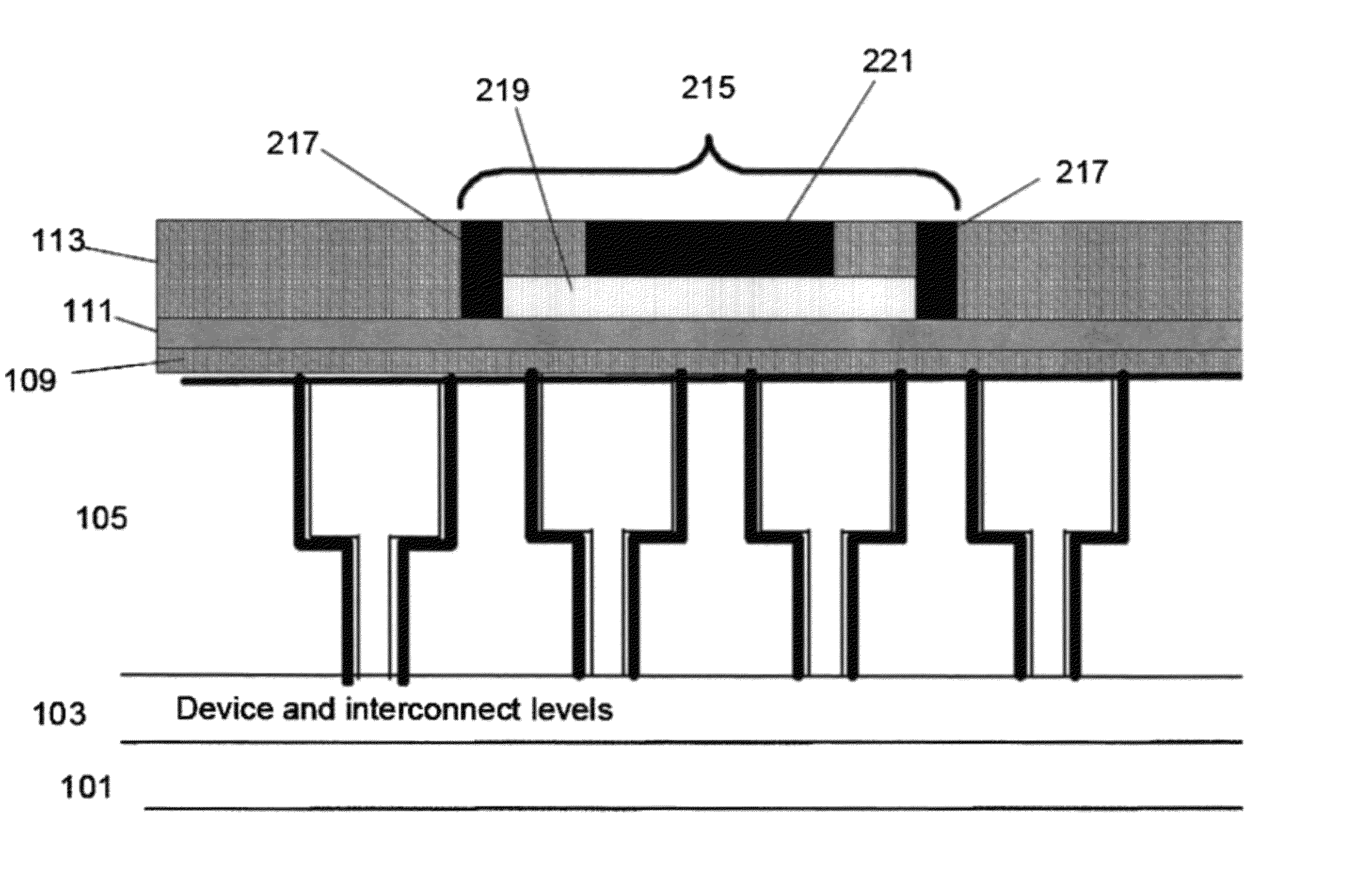
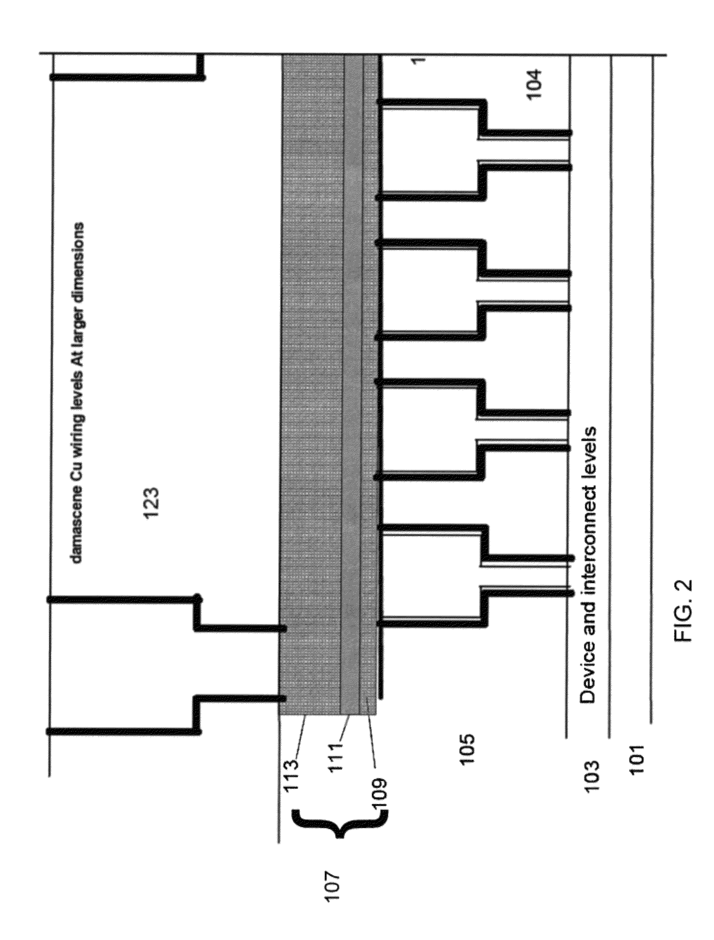
[0047]The invention will now be described with reference to the drawing figures, in which like reference numerals refer to like parts throughout. It is emphasized that, according to common practice, the various features of the drawing are not necessary to scale. On the contrary, the dimensions of the various features can be arbitrarily expanded or reduced for clarity. Exemplary embodiments are provided below for illustration purposes and do not limit the claims.

[0048]The exemplary disclosure describes, at least in part but not limited to, creating an integrated circuit with two or more levels of active device, whereas the related art has one level. In the related art, two independent layers are bonded together, whereas in the present exemplary disclosure there is a building in a stepwise fashion and using a single substrate. In the related art, two layers can be fabricated independently and then bonded together. Therefore, in the exemplary embodiments, there is a building of the mul...


PUM


Abstract

A monolithic integrated circuit and method includes a substrate, a plurality of semiconductor device layers monolithically integrated on the substrate, and a metal wiring layer with vias interconnecting the plurality of semiconductor device layers. The semiconductor device layers are devoid of bonding or joining interface with the substrate. A method of fabricating a monolithic integrated circuit using a single substrate, includes fabricating semiconductor devices on a substrate, fabricating at least one metal wiring layer on the semiconductor devices, forming at least one dielectric layer in integral contact with the at least one metal wiring layer, forming contact openings through the at least one dielectric layer to expose regions of the at least one metal wiring layer, integrally forming, from the substrate, a second semiconductor layer on the dielectric layer, and in contact with the at least one metal wiring layer through the contact openings, and forming a plurality of non-linear semiconductor devices in said second semiconductor layer.

Description

BACKGROUND OF THE INVENTION[0001]1. Field of the Invention[0002]The disclosed invention relates generally to fabrication of integrated circuits, and more particularly, but not by way of limitation, to wiring levels on an integrated circuit in a back-end-of-line (BEOL) processing that include active and / or nonlinear devices embedded therein.[0003]2. Description of the Related Art[0004]From the beginning of semiconductor manufacture, there has been a progressive trend to miniaturizing electrical components through dimension scaling, thereby resulting in increased circuit density over time. In the general manufacturing scheme of an integrated circuit (IC), there are two major parts, the front end of line (FEOL) processing and the back end of line (BEOL) processing.[0005]In general, the FEOL layer contains active and nonlinear devices requiring a semiconductor, such as transistors, diodes, varactors, photodetectors, photo-emitters, polysilicon resistors, MOS (metal-oxide-silicon or meta...

Claims


Application Information

Patent Timeline
07 Jan 2014
Publication
US8624323B2
IPC
H01L23/48; H01L23/34; H01L29/40; H01L29/94; H01L29/76
CPC
H01L29/66984; H01L27/016; H01L23/5228; H01L27/0688; H01L23/53238; H01L29/872; H01L23/5223; H01L29/861
Inventors
GATES, STEPHEN M.; EDELSTEIN, DANIEL C.