
Semiconductor device

a technology of semiconductor chips and semiconductors, applied in the direction of solid-state devices, basic electric elements, metal-patterned materials, etc., can solve problems such as cracks in semiconductor chips, and achieve the effect of preventing damage and reducing the linear expansion coefficient in the thickness direction of the substra

Inactive Publication Date: 2014-01-14
SUMITOMO BAKELITE CO LTD
View PDF23 Cites 1 Cited by
  • Summary
  • Abstract
  • Description
  • Claims
  • Application Information

AI Technical Summary

Benefits of technology

This patent addresses a technical problem related to semiconductor device warping caused by thermal history. The solution involves using a core layer with low expansion to reduce the strain on the substrate and prevent damage to the semiconductor elements and interfaces during use. Ultimately, this improves the overall quality and reliability of the semiconductor device.

Problems solved by technology

In a conventional semiconductor device, such warpage would cause damage such as cracks in the semiconductor chip, at the interface between the semiconductor chip and a bump, and at the interface between the bump and the substrate, in some cases.

Method used


Image

  • Semiconductor device
  • Semiconductor device
  • Semiconductor device

Examples


example 1-1

[0159]Preparation of Resin Composition: Bisphenol F Epoxy Resin with an epoxy equivalent of 165 (11 parts by weight), N-[2-methyl-4-(oxiranylmethoxy)phenyl]-N-(oxiranylmethyl)oxiranemethanamine (ELM-100 made by Sumitomo Chemical) (11 parts by weight), 4,4′-methylenbis-(2-ethylanilin) (Kayahard AA made by Nippon Kayaku Co. Ltd.) (10 parts by weight), γ-glycidylpropyltriethoxysilane (KBE403 made by Shin-Etsu Chemical Co., Ltd.) (1 part by weight), spherical fused silica with an average particle diameter of 0.5 μm (SO-25R made by Admatechs Corporation Limited) (65 parts by weight) were weighed, kneaded through a three-roll mill, and the blend was defoamed under vacuum to prepare a liquid resin composition.

example 1-2

[0160]A resin composition was prepared as in Example 1-1 except that the formulation of the resin composition was changed as follows:

[0161]Bisphenol F epoxy resin with an epoxy equivalent of 165 (18 parts by weight), N-[2-methyl-4-(oxiranylmethoxy) phenyl]-N-(oxiranylmethyl)oxiranemethanamine (ELM-100 made by Sumitomo Chemical) (6 parts by weight), and 4,4′-methylenbis-(2-ethylanilin) (Kayahard AA made by Nippon Kayaku Co. Ltd.) (10 parts by weight) were used.

example 1-3

[0162]A resin composition was prepared as in Example 1-1 except that the formulation of the resin composition was changed as follows:

[0163]Bisphenol F epoxy resin with an epoxy equivalent of 165 (25 parts by weight) and 4,4′-methylenbis-(2-ethylanilin) (Kayahard AA made by Nippon Kayaku Co. Ltd.) (8 parts by weight) were used. N-[2-methyl-4-(oxiranylmethoxy)phenyl]-N-(oxiranylmethyl) oxiranemethanamine (ELM-100 made by Sumitomo Chemical) was not used.


PUM


Abstract

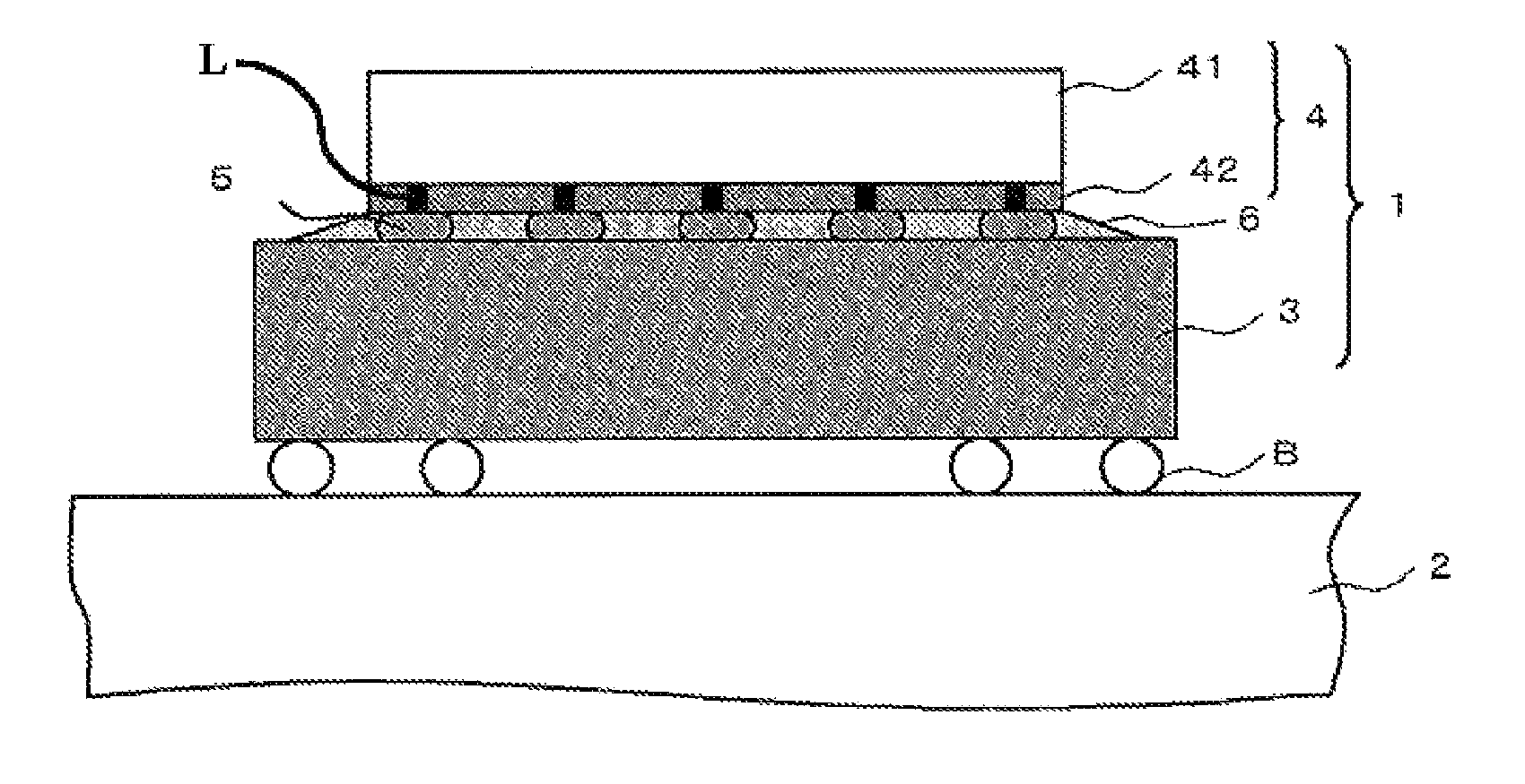
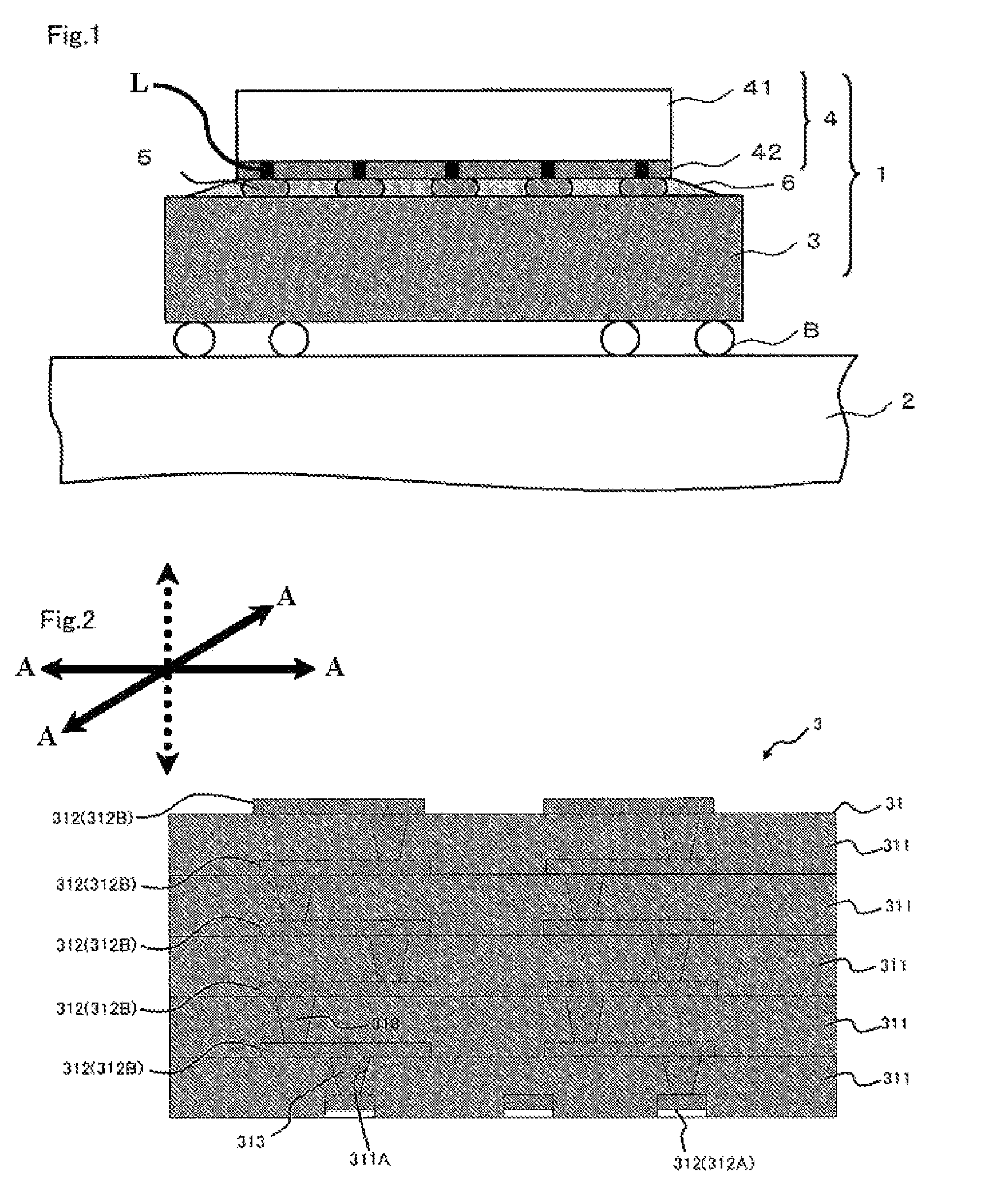
The semiconductor device 1 includes a substrate 3, a semiconductor chip 4 mounted on the substrate 3, the substrate 3, a bump 5 connecting the substrate 3 and the semiconductor chip 4, and an underfill 6 filling in around the bump 5. In the case of a bump 5 composed of a high-melting-point solder having a melting point of 230° C. or more, the underfill 6 is composed of a resin material having an elastic modulus in the range of 30 MPa to 3000 MPa. In the case of a bump 5 composed of a lead-free solder, the underfill 6 is composed of a resin material having an elastic modulus in the range of 150 MPa to 800 MPa. An insulating layer 311 of buildup layers 31 of the substrate 3 has a linear expansion coefficient of 35 ppm / ° C. or less in the in-plane direction of the substrate at temperatures in the range of 25° C. to the glass transition temperature.

Description

TECHNICAL FIELD[0001]The present invention relates to a semiconductor device.BACKGROUND ART[0002]In face-down mounting of a semiconductor chip (semiconductor element) on a substrate, an undesirable gap is formed between the substrate and the semiconductor chip. The gap must be filled with an insulating material called underfill. Thermosetting resins such as epoxy resins have been widely used as materials for the underfill (Patent Document 1).[0003][Patent Document 1] Japanese Unexamined Patent Application Publication No. H11-233571DISCLOSURE OF INVENTION[0004]In general, substrates and semiconductor chips have different linear expansion coefficients. The substrates, composed of materials containing organic resins, have linear expansion coefficients larger than that of the semiconductor chips. When a semiconductor device including a semiconductor chip mounted on a substrate undergoes thermal history, the substrate warps due to a difference in linear expansion coefficient between them...

Claims


Application Information

Patent Timeline
Patent Type & Authority Patents(United States)
IPC IPC(8): H01L29/40H01L23/52H01L23/48
CPCH01L21/563H01L21/6835H01L23/293H01L2224/32225H01L2924/01079H01L2924/30105H01L2924/15311H01L2924/01077H01L2221/68345H01L2924/01087H01L24/16H01L2924/01322H01L2224/73204H01L2924/01078H01L2224/73203H01L2924/01019H01L2224/16225H01L2924/12042H01L2924/00014H01L2924/00011H01L2924/00H01L2224/0401H01L23/12H01L23/29H01L23/31
Inventor SUGINO, MITSUOHOSOMI, TAKESHIWADA, MASAHIROARAI, MASATAKA
Owner SUMITOMO BAKELITE CO LTD
Learn More