Method, system and program storage device for modeling the capacitance associated with a diffusion region of a silicon-on-insulator device

a technology of silicon-on-insulator and diffusion region, which is applied in the field of model parasitic capacitance associated with the diffusion region of the silicon-on-insulator device, can solve problems such as affecting and achieve the effect of accurately simulating the performance of the soi devi

Inactive Publication Date: 2014-01-14
GLOBALFOUNDRIES US INC
View PDF12 Cites 3 Cited by
  • Summary
  • Abstract
  • Description
  • Claims
  • Application Information

AI Technical Summary

Benefits of technology

[0006]More particularly, disclosed herein are embodiments of a computer-implemented method for modeling parasitic capacitance associated with a diffusion region of a silicon-on-insulator (SOI) device. The method can comprise analyzing an integrated circuit design layout in order to at least (1) identify side edges of the diffusion region that are capacitively coupled to adjacent conductive structures and (2) determine distances from each of the side edges to the adjacent conductive structures. Then, a formula for determining a parasitic capacitance (CD-S) between the diffusion region and a substrate below the diffusion region can be developed. This formula for CD-S can be developed so that it has an area component and a perimeter component and further so that the perimeter component takes into consideration proximity to adjacent conductive structures. Specifically, the perimeter component can have a side edge component and, if applicable, a corner component and both the side edge and corner components can be based on previously determined distances between the side edges of the diffusion region and the adjacent conductive structures. Once the formula for CD-S is developed, it can be used to determine CD-S. Specifically, such a formula can, for example, be used by SOI device models and parasitic extraction tools, which determine parasitics and generate a SPICE (Simulation Program with Integrated Circuit Emphasis) netlist based a circuit layout. Optionally, the method embodiment can further comprise developing formulas for second parasitic capacitances (CD-D) between the diffusion region and each of the adjacent conductive structures, based on the previously established distances between the side edges of the diffusion region and the adjacent conductive structures. Specifically, like the formula for CD-S mentioned above, the formulas for CD-D can, for example, be used by SOI device models and parasitic extraction tools, which determine parasitics and generate a SPICE (Simulation Program with Integrated Circuit Emphasis) netlist based a circuit layout. Thus, the capacitance CD-S between the diffusion region and the substrate and, if determined, the capacitances CD-D between the diffusion region and each of the adjacent structures can then be used to more accurately simulate the performance of the SOI device.
[0007]Also, disclosed herein are embodiments of a computer system for modeling parasitic capacitance associated with a diffusion region of a silicon-on-insulator (SOI) device. The computer system embodiments can comprise a memory and at least one processor. The memory can store an integrated circuit design layout. The processor(s) can comprise at least a layout analyzer, a capacitance formula generator and a capacitance calculator. The layout analyzer can access the layout and can analyze it in order to at least (1) identify side edges of the diffusion region that are capacitively coupled to adjacent conductive structures and (2) determine distances from each of the side edges to the adjacent conductive structures. Then, the capacitance formula generator can develop a formula for determining a parasitic capacitance (CD-S) between the diffusion region and a substrate below the diffusion region. This formula for CD-S can be developed by the generator so that it has an area component and a perimeter component and further so that the perimeter component takes into consider proximity to adjacent conductive structures. Specifically, the perimeter component can have a side edge component and, if applicable, a corner component and both the side edge and corner components can be based on previously determined distances between the side edges of the diffusion region and the adjacent conductive structures. Once the formula for CD-S is developed by the capacitance formula generator, it can be used by the capacitance calculator to determine CD-S. Specifically, such a formula can, for example, be used by SOI device models and parasitic extraction tools, which determine parasitics and generate a SPICE (Simulation Program with Integrated Circuit Emphasis) netlist based a circuit layout. Optionally, the capacitance formula generator can also generate formulas for calculating second parasitic capacitances (CD-D) between the diffusion region and each of the adjacent conductive structures based on the previously established distances between the side edges of the diffusion region and the adjacent conductive structures. Once the formulas for the capacitances CD-D are developed by the capacitance formula generator, they can be used by the capacitance calculator to determine the capacitances CD-D. Specifically, like the formula for CD-S mentioned above, the formulas for CD-D can, for example, be used by SOI device models and parasitic extraction tools, which determine parasitics and generate a SPICE (Simulation Program with Integrated Circuit Emphasis) netlist based a circuit layout. Thus, the capacitance CD-S between the diffusion region and the substrate and, if determined, the capacitances CD-D between the diffusion region and each of the adjacent structures can then be used by a simulator to more accurately simulate the performance of the SOI device.

Problems solved by technology

Such parasitic capacitances can greatly impact SOI device performance.
However, the current techniques used to model may result in error.

Method used


Image

  • Method, system and program storage device for modeling the capacitance associated with a diffusion region of a silicon-on-insulator device
  • Method, system and program storage device for modeling the capacitance associated with a diffusion region of a silicon-on-insulator device
  • Method, system and program storage device for modeling the capacitance associated with a diffusion region of a silicon-on-insulator device

Examples


Embodiment Construction

[0017]The embodiments and the various features and advantageous details thereof are explained more fully with reference to the non-limiting embodiments that are illustrated in the accompanying drawings and detailed in the following description.

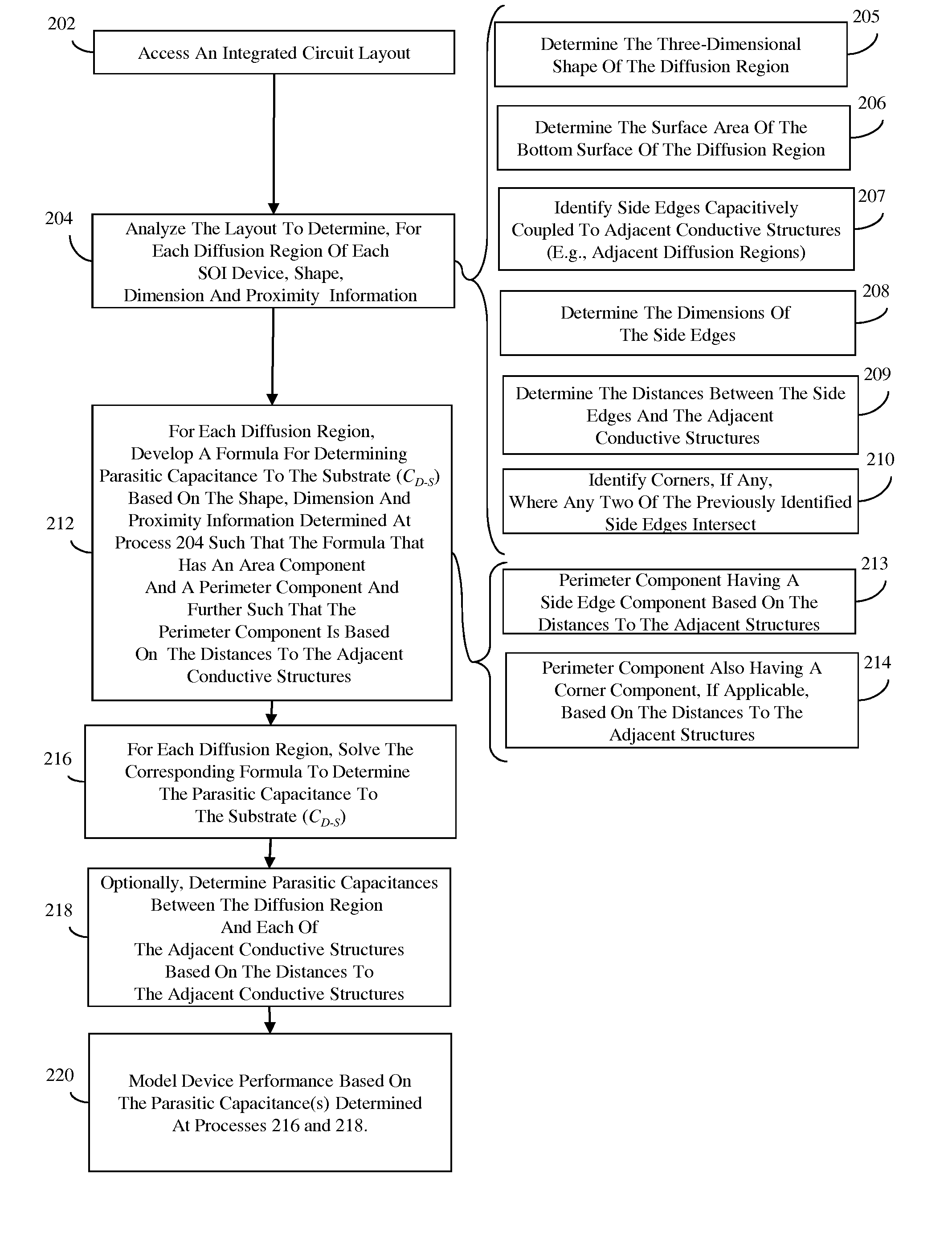
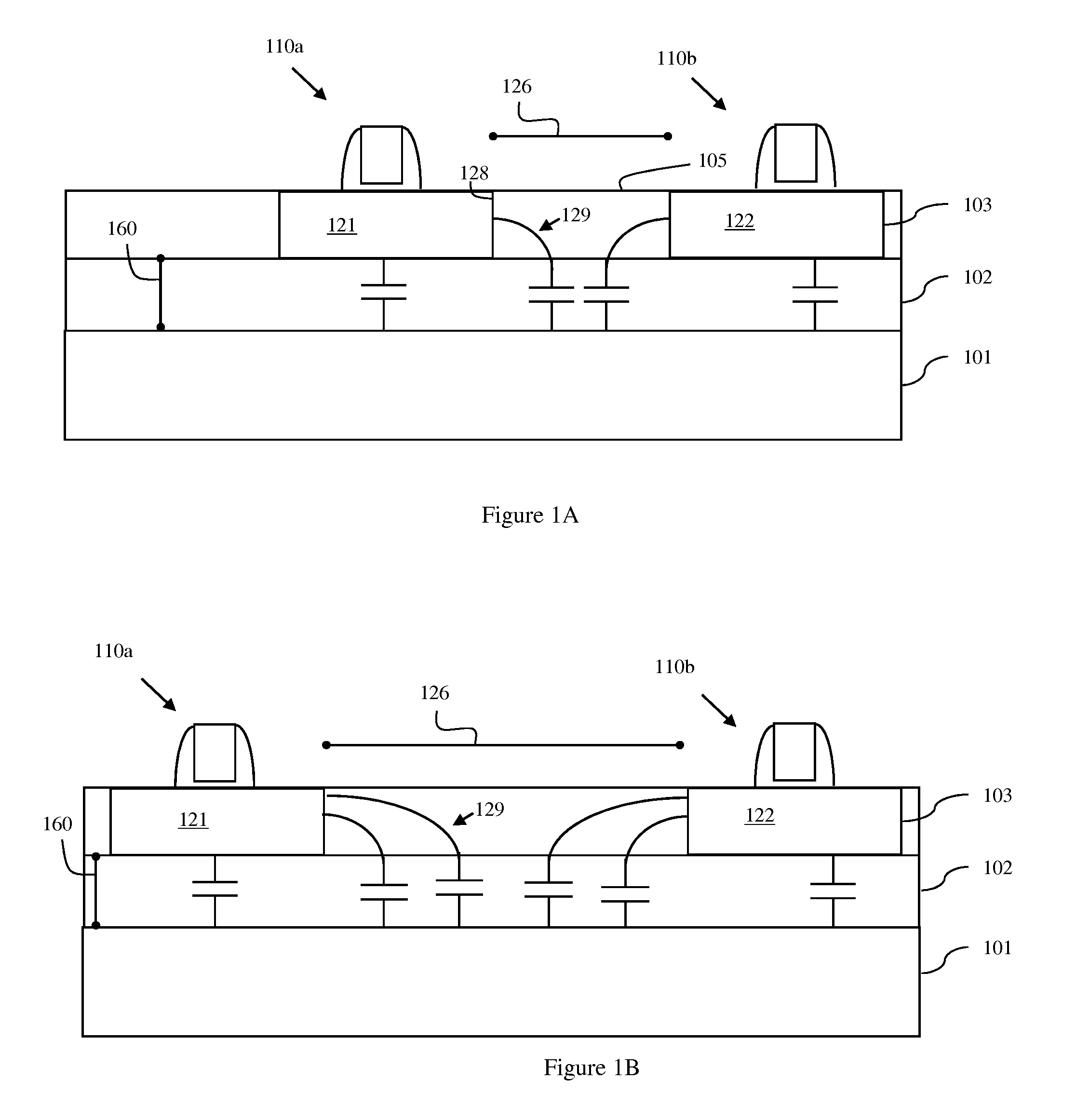
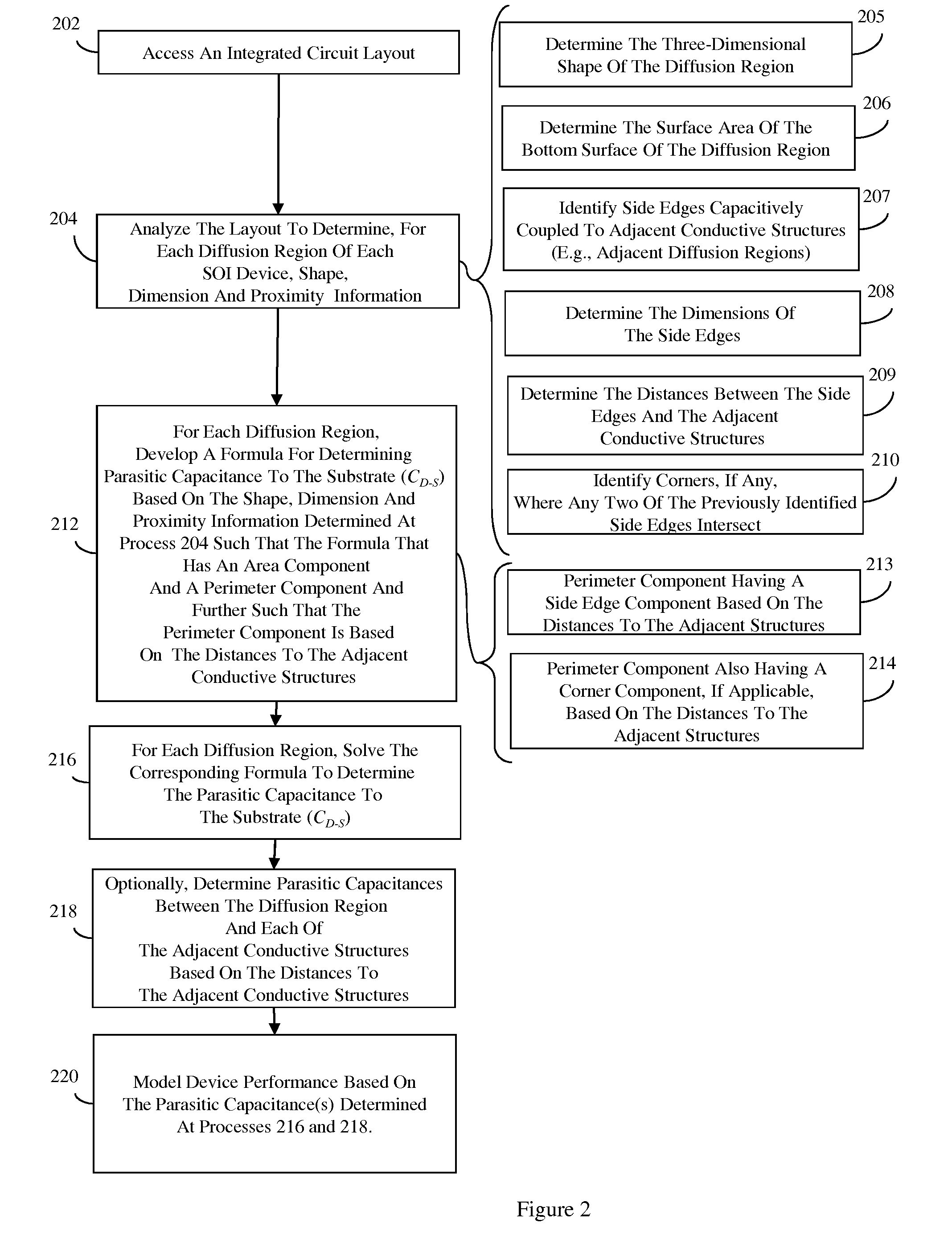
[0018]As mentioned above, parasitic capacitances associated with a diffusion region of a silicon-on-insulator (SOI) device (e.g., a source / drain region of a metal oxide semiconductor field effect transistor (MOSFET), a diffusion region of a metal oxide semiconductor (MOS) capacitor, etc.) can include, for example, the capacitance between that diffusion region and the substrate below (CD-S) as well as capacitances between that diffusion region and any adjacent conductive structures (CD-D) (e.g., any adjacent diffusion regions of other SOI devices). Such parasitic capacitances can greatly impact SOI device performance. Thus, during SOI device design, accurate modeling of parasitic capacitances associated with each diffusion region is very import...


PUM


Abstract

Disclosed are embodiments of a method, system and program storage device for accurately modeling parasitic capacitance(s) associated with a diffusion region of a silicon-on-insulator (SOI) device and doing so based, at least in part, on proximity to adjacent conductive structures. In these embodiments, the layout of an integrated circuit design can be analyzed to determine, for the diffusion region, shape, dimension and proximity information. Then, a formula can be developed and used for determining the parasitic capacitance between the diffusion region and the substrate below (CD-S). This formula can have a perimeter component, including a side edge component and, if applicable, a corner component, both of which account for the fact that CD-S is generally dependent on the distances between the diffusion region and any adjacent conductive structures. Additionally, the parasitic capacitance between the diffusion region and any adjacent conductive structure (CD-D) can be determined based on such distances.

Description

BACKGROUND[0001]1. Field of the Invention[0002]The embodiments disclosed herein relate to modeling parasitic capacitances associated with a diffusion region of a silicon-on-insulator (SOI) device and, more particularly, to a method, a computer system, and a program storage device for modeling parasitic capacitances associated with a diffusion region (e.g., diffusion region to substrate capacitance and diffusion region to adjacent diffusion region capacitance) as a function of the distance between the diffusion region and the adjacent diffusion region(s).[0003]2. Description of the Related Art[0004]Parasitic capacitances associated with a diffusion region of a silicon-on-insulator (SOI) device (e.g., a source / drain region of a metal oxide semiconductor field effect transistor (MOSFET), a diffusion region of a metal oxide semiconductor (MOS) capacitor, etc.) can include, for example, the capacitance between that diffusion region and the substrate below as well as capacitances between ...

Claims


Application Information

Patent Timeline
Patent Type & Authority Patents(United States)
IPC IPC(8): G06F17/50
CPCG06F17/5081G06F17/5036G06F30/398G06F30/367
Inventor LU, NING
Owner GLOBALFOUNDRIES US INC
Why Eureka
Try Eureka