Process for cleaning semiconductor devices and/or tooling during manufacturing thereof

Active Publication Date: 2014-02-11
GLOBALFOUNDRIES US INC
View PDF25 Cites 8 Cited by
  • Summary
  • Abstract
  • Description
  • Claims
  • Application Information

AI Technical Summary

Benefits of technology

The patent describes processes for cleaning semiconductor devices and tools during manufacture. The processes involve using an antioxidant to form an insoluble adduct with residues from the device or tool, and then a base to solubilize the adduct. This leads to the removal of ceria particles from chemical mechanical processing tools. The technical effect is improved cleaning of semiconductor materials during manufacturing.

Problems solved by technology

These structures are fragile due to their increasingly small dimensions and the types of materials used to form the structures.
Often BEOL processing includes one or more chemical mechanical planarization (CMP) process steps, which are inherently very dirty processes.
However, the semiconductor devices as well as the CMP pads / brushes are often contaminated with particles of ceria that require removal for successful and efficient device manufacture.
In FEOL processes, the typical cleaning chemistries are not selective enough to differentiate between some of these residues that must be removed or metals and the metals required to remain.
TiN is used as a component of some metal gate structures and any loss of TiN in these metal gate structures can result in an undesirable decrease or change in device performance.

Method used


Image

  • Process for cleaning semiconductor devices and/or tooling during manufacturing thereof
  • Process for cleaning semiconductor devices and/or tooling during manufacturing thereof

Examples


Embodiment Construction

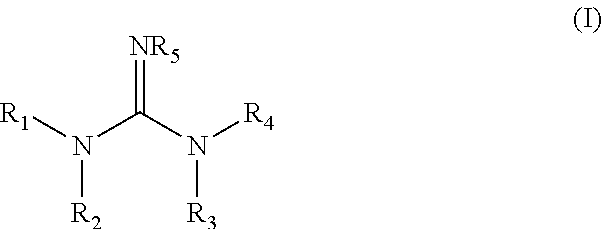
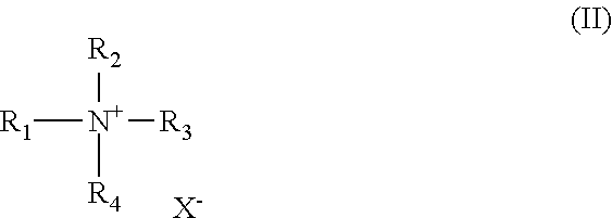
[0010]Disclosed herein are aqueous cleaning processes and compositions for cleaning substrates during semiconductor manufacturing and / or semiconductor tooling surfaces. The processes generally include sequentially exposing the substrate to a first aqueous solution of an antioxidant compound and then to a second solution that is a basic aqueous solution. It is understood that the first and second aqueous solutions by definition uses purified water as the solution solvent. Additionally, the antioxidant compound can be selected to possess both antioxidant and reductant properties. Surprisingly, while separate exposure of the contaminate to either the antioxidant aqueous solution or the basic aqueous solution by themselves results in insoluble precipitates, the sequential process as described herein results in the dissolution and / or complexation solubilization of the undesired contaminate. Thus, this treatment in a sequence of solutions advantageously results in the removal of our undes...


PUM

PropertyMeasurementUnit
Temperatureaaaaaaaaaa
Fractionaaaaaaaaaa

Abstract

Cleaning processes for cleaning semiconductor devices or semiconductor tooling during manufacture thereof generally include contacting the semiconductor devices or semiconductor tooling with an antioxidant to form an insoluble adduct followed by solubilizing the adduct with a basic aqueous cleaning solution.

Description

BACKGROUND[0001]The present disclosure generally relates to semiconductor device manufacturing and, more particularly, to the cleaning and removal of residues and / or contaminants formed on the semiconductor device during manufacture.[0002]The integrated circuit manufacturing process can generally be divided into front end of line (FEOL) and back end of line (BEOL) processing. The FEOL processes are focused on fabrication of the different devices that make up the integrated circuit, whereas BEOL processes are focused on forming metal interconnects between the different devices of the integrated circuit. In the FEOL processes, shallow trench isolation structures and gate or memory stacks are typically formed. These structures are fragile due to their increasingly small dimensions and the types of materials used to form the structures. BEOL processes may also have fragile structures such as dual damascene etched openings in low k dielectric materials or polysilicon interconnect lines. ...

Claims


Application Information

Patent Timeline
IPC IPC(8): B08B3/04
CPCB24B53/017H01L21/02052B08B3/04H01L21/02057
Inventor CHHABRA, VISHALFITZSIMMONS, JOHN A.KHOJASTEH, MAHMOUDMUNCY, JENNIFER
Owner GLOBALFOUNDRIES US INC
Why Eureka
Try Eureka