Method for manufacturing semiconductor device and display device
a technology of semiconductor devices and display devices, applied in the field of display devices, can solve the problems of increasing cost, reducing yield, and complicated process of polycrystalline semiconductor films, and achieve the effect of improving the mass productivity of display devices including thin film transistors using microcrystalline semiconductor films and increasing the film-formation rate of microcrystalline semiconductor films
- Summary
- Abstract
- Description
- Claims
- Application Information
AI Technical Summary
Benefits of technology
Problems solved by technology
Method used
Image
Examples
embodiment mode 1
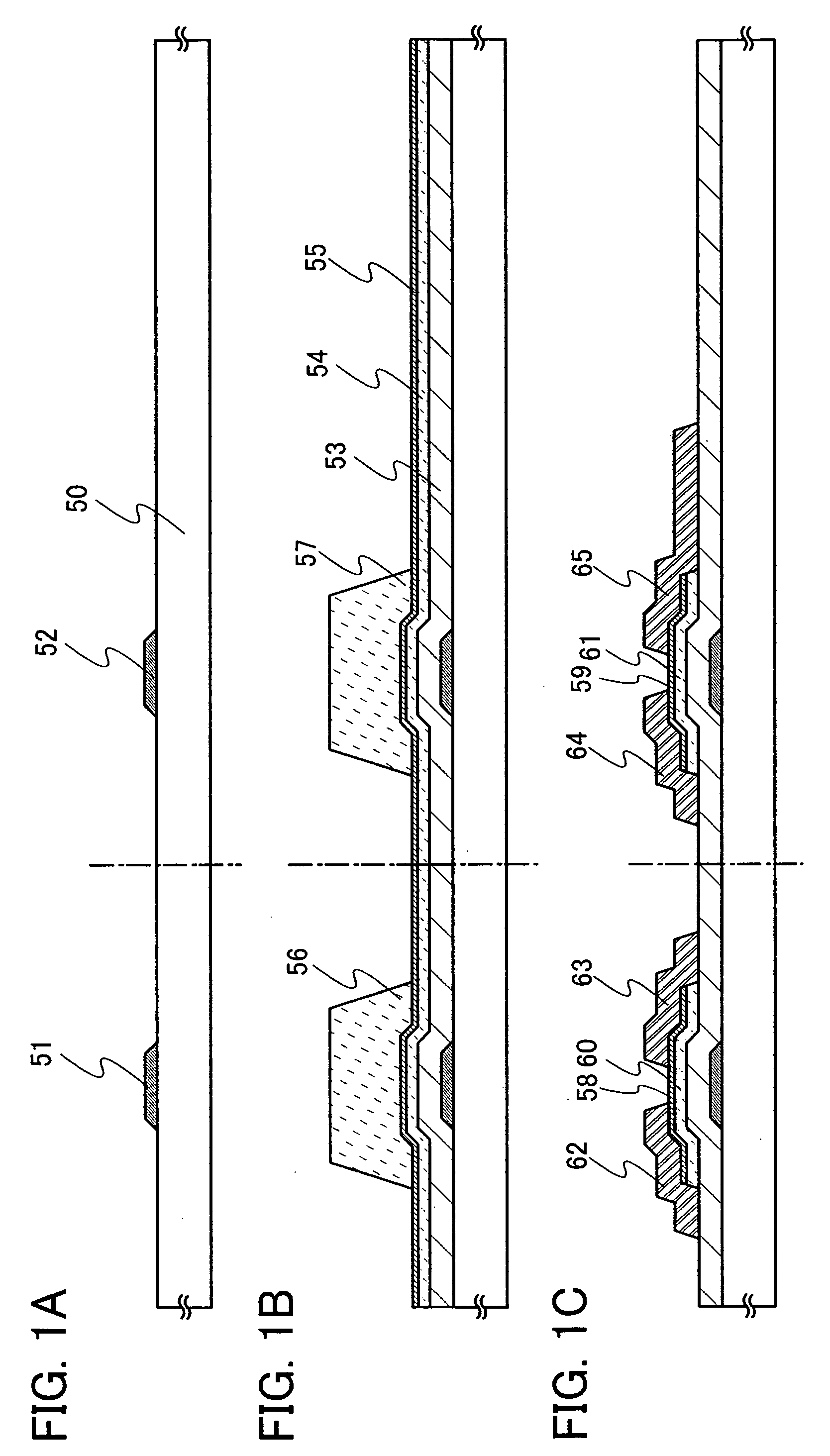
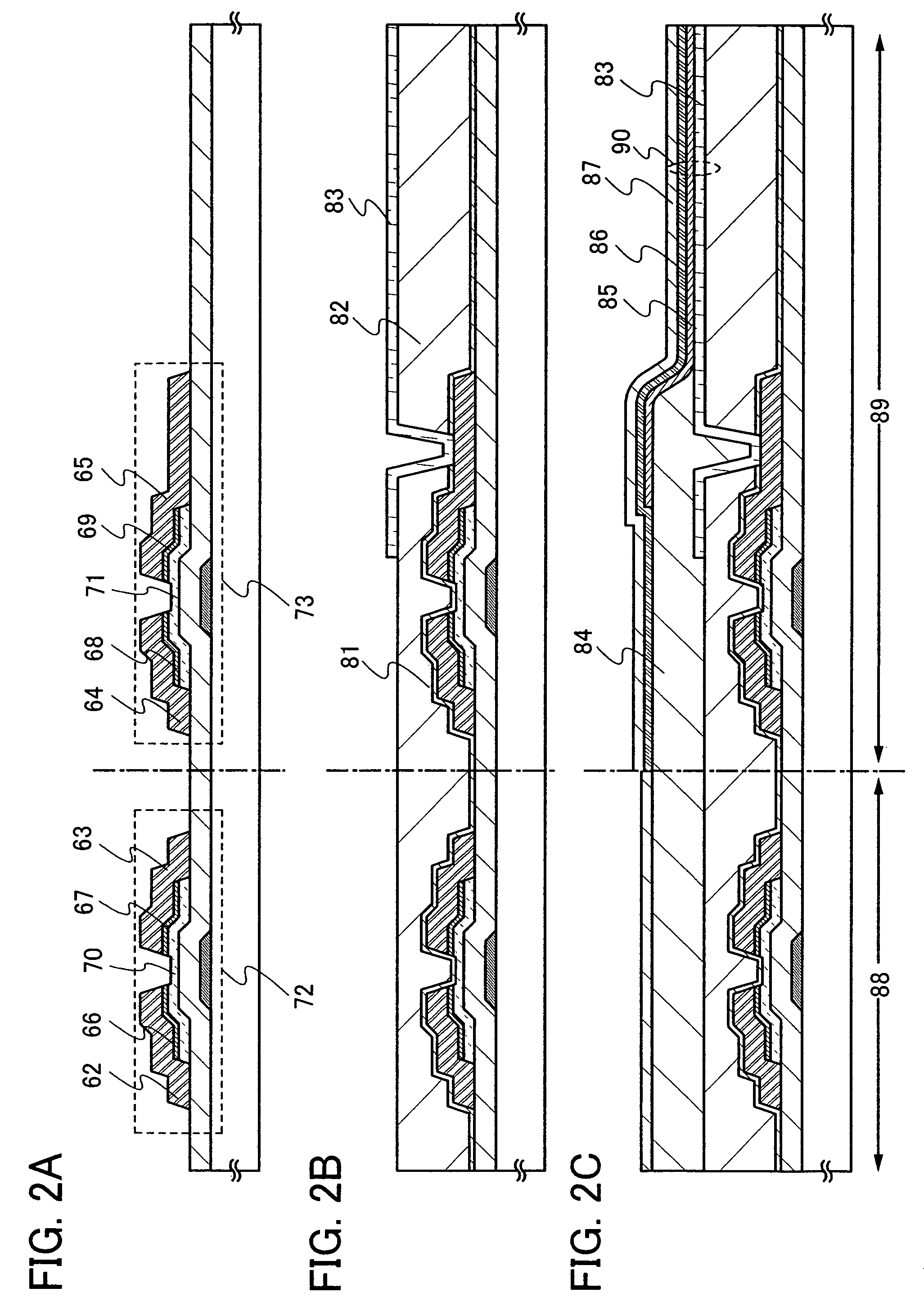
[0033]A method for manufacturing a display device of the present invention will be described. First, the description is made using a light-emitting device that is one mode of the display device. FIGS. 1A to 3C are cross-sectional views each illustrating a thin film transistor used for a driver circuit and a thin film transistor used for a pixel portion. As for a thin film transistor in which a microcrystalline semiconductor film is used, an n-type thin film transistor has higher mobility than a p-type thin film transistor; thus, an n-type thin film transistor is more suitable for a driver circuit. However, in the present invention, either an n-type or p-type thin film transistor can be used. With any polarity of a thin film transistor, it is preferable that all the thin film transistors formed over one substrate have the same polarity so that the number of manufacturing steps is reduced.
[0034]As illustrated in FIG. 1A, gate electrodes 51 and 52 are formed over a substrate 50. As the...
embodiment mode 2
[0109]This embodiment mode will describe another structure of the thin film transistor shown in Embodiment Mode 1 with reference to FIG. 12.
[0110]Thin film transistors 72 and 73 described in this embodiment mode has a feature that, as illustrated in FIG. 12, end portions of source electrodes 62a and 64a and end portions of source regions 66 and 68 are not in alignment, and end portions of drain electrodes 63a and 65a and end portions of drain regions 67 and 69 are not in alignment.
[0111]In this embodiment mode, using the same resist mask, a conductive film is etched by wet etching to form the source and drain electrodes 62a to 65a, and a semiconductor film to which an impurity element imparting one conductivity type is added is etched by dry etching to form the source and drain regions 66 to 69. With the structure of the source and drain electrodes 62a to 65a in this embodiment mode, the distance between the facing electrodes is widened; therefore, short-circuit between the source a...
embodiment mode 3
[0112]This embodiment mode will describe a structure of a display panel which is one mode of the display device of the present invention.
[0113]FIG. 9 illustrates a mode of a display panel in which a pixel portion 6012 formed over a substrate 6011 is connected to a signal line driver circuit 6013 which is separately formed. The pixel portion 6012 and a scanning line driver circuit 6014 are each formed using a thin film transistor which uses a microcrystalline semiconductor film. By forming the signal line driver circuit with a thin film transistor by which higher mobility can be obtained compared to a thin film transistor using the microcrystalline semiconductor film, operation of the signal line driver circuit which demands a higher driving frequency than that of the scanning line driver circuit can be stabilized. Note that the signal line driver circuit 6013 may be formed using a thin film transistor using a single-crystalline semiconductor, a thin film transistor using a polycryst...
PUM
 Abstract
Description
Claims
Application Information


