Method for fabricating first and second epitaxial cap layers

a technology of epitaxial cap and electrode, which is applied in the direction of semiconductor devices, basic electric elements, electrical appliances, etc., can solve the problems of non-uniform thickness of resultant silicon germanium (sige), mismatches of device performance, etc., to improve device performance mismatches, lessen turn-off currents, and enhance the effect of turn-on currents

Active Publication Date: 2014-02-11
MARLIN SEMICON LTD
View PDF139 Cites 17 Cited by
  • Summary
  • Abstract
  • Description
  • Claims
  • Application Information

AI Technical Summary

Benefits of technology

[0007]The present invention is directed to a MOS device, capable of enhancing turn-on currents and lessening turn-off currents, so that the mismatches of the device performance can be ameliorated.
[0008]The present invention is directed to a method for fabricating a MOS device, wherein alterations in the fabrication process can achieve enhancement of the turn-on currents, decrease in the turn-off currents, and improvement in the mismatches of the device performance.
[0032]As mentioned above, the MOS device in this invention can enhance the turn-on currents and lessen the turn-off currents, thereby improving the mismatches of the device performance. Moreover, the fabricating method of the MOS device in this invention is capable of enhancing the turn-on currents, lessening the turn-off currents, and improving the mismatches of the device performance through modifications in the fabrication process.

Problems solved by technology

Accordingly, the thickness of the resultant silicon germanium (SiGe) is non-uniform (i.e. so-called loading effects), and issues regarding mismatches of the device performance arise therefrom.

Method used


Image

  • Method for fabricating first and second epitaxial cap layers
  • Method for fabricating first and second epitaxial cap layers
  • Method for fabricating first and second epitaxial cap layers

Examples


Embodiment Construction

[0037]Reference will now be made in detail to the present preferred embodiments of the invention, examples of which are illustrated in the accompanying drawings. Wherever possible, the same reference numbers are used in the drawings and the description to refer to the same or like parts.

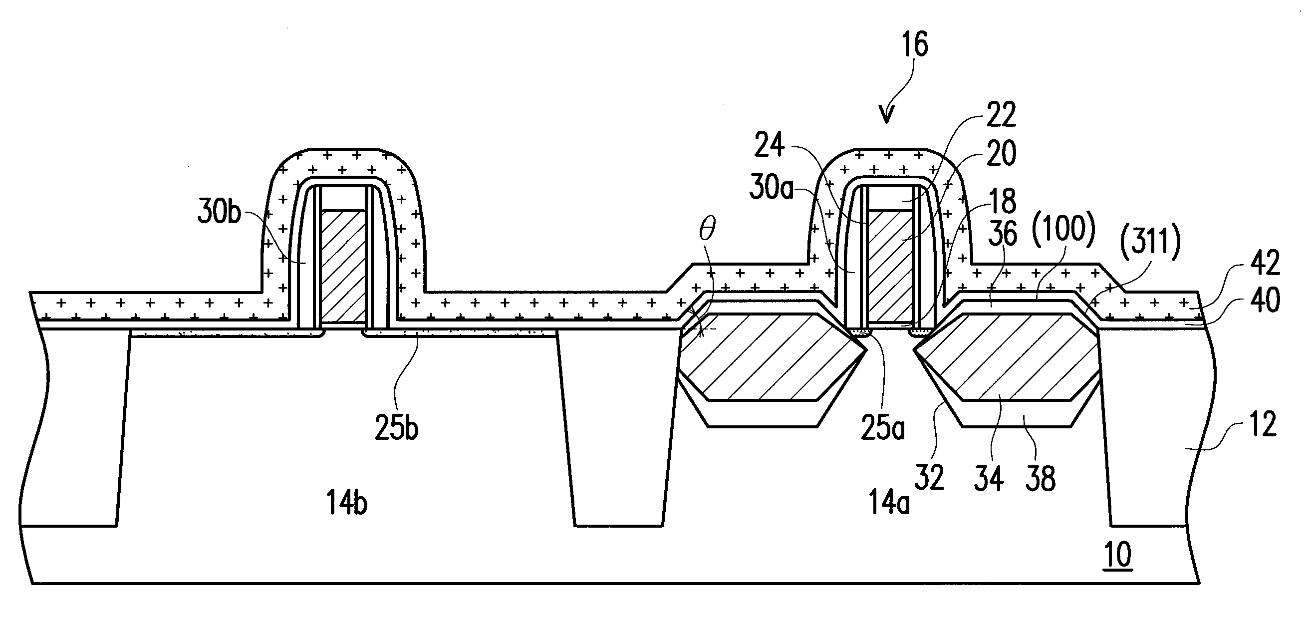
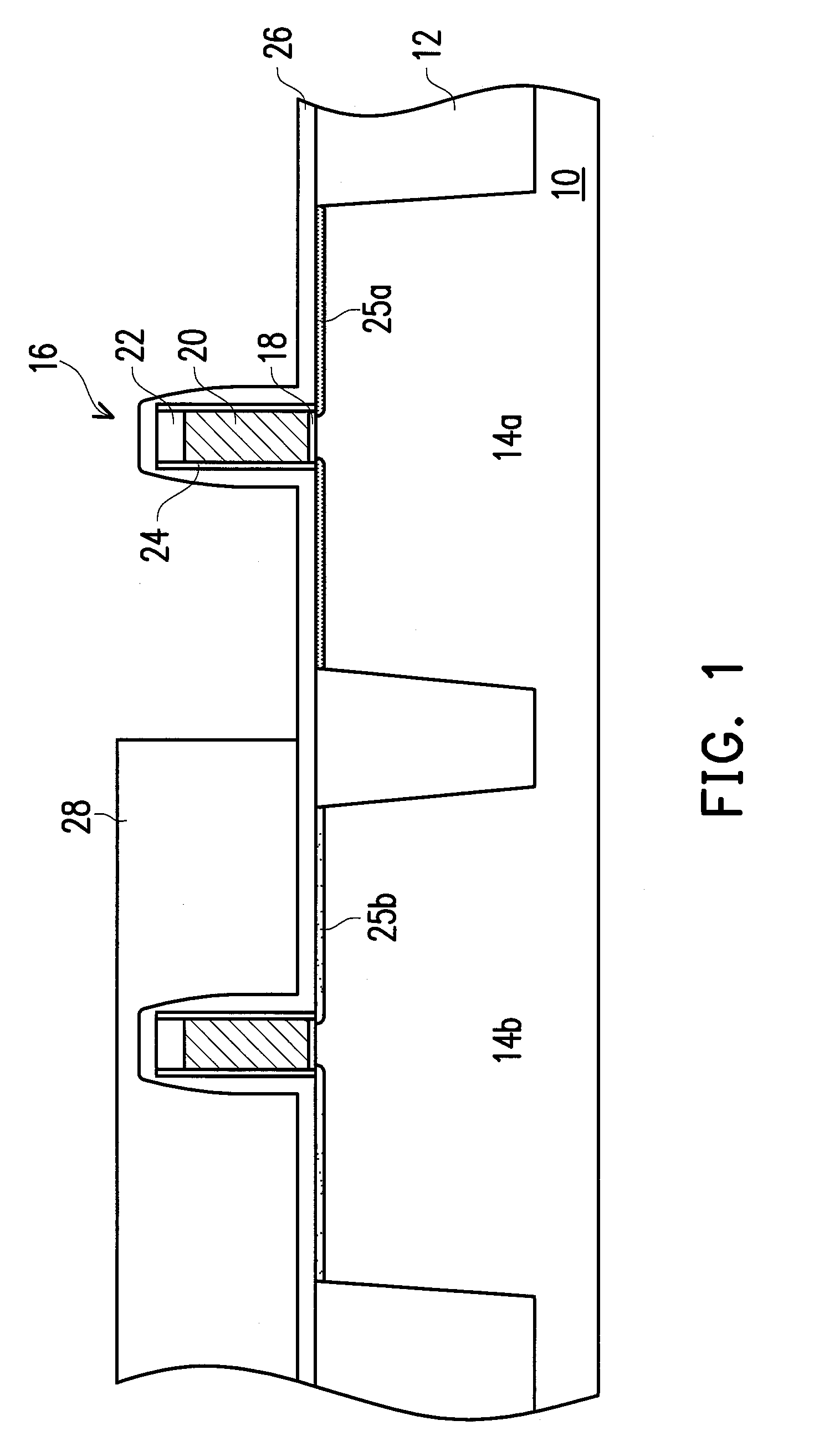
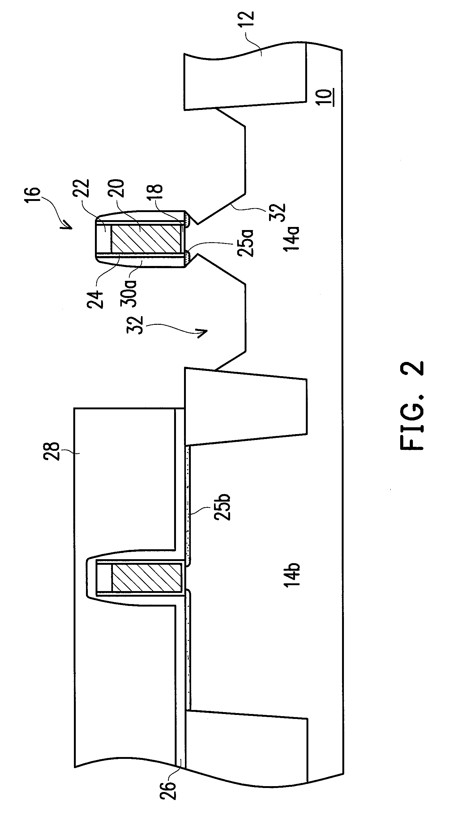
[0038]FIGS. 1-7 depict, in a cross-sectional view, a method for fabricating a MOS device according to an embodiment of the present invention.

[0039]Referring to FIG. 1, isolation structures 12 are formed in a substrate 10, so as to define a first active area 14a and a second active area 14b. The material of the substrate 10 includes semiconductor, such as silicon. The material of the isolation structures 12 includes insulating material, such as silicon oxide. The isolation structures 12 are, for example, formed by a shallow trench isolation (STI) method.

[0040]Stack structures are then formed on the first and the second active areas 14a, 14b of the substrate 10, respectively. Each stack structure 16 in...


PUM

PropertyMeasurementUnit
included angleaaaaaaaaaa
epitaxial temperatureaaaaaaaaaa

Abstract

A method for fabricating a metal oxide semiconductor (MOS) device is described, including following steps. Two recesses are formed in a substrate. A first epitaxy growth process is performed, so as to form a first semiconductor compound layer in each of the recesses. A second epitaxy growth process is performed with an epitaxial temperature lower than 700° C., so as to form a cap layer on each of the first semiconductor compound layers. Each of the cap layers includes a second semiconductor compound layer protruding from a surface of the substrate. The first and the second semiconductor compound layers are composed of a first Group IV element and a second Group IV element, wherein the second Group IV element is a nonsilicon element. The content of the second Group IV element in the second semiconductor compound layers is less than that in the first semiconductor compound layers.

Description

BACKGROUND OF THE INVENTION[0001]1. Field of the Invention[0002]The present invention relates to a metal oxide semiconductor (MOS) device and a method for fabricating the same.[0003]2. Description of Related Art[0004]Metal oxide semiconductor (MOS) transistor is one of the most common elements used in many different semiconductor devices, such as memories, image sensors or displays. A typical MOS includes a silicon oxide dielectric layer, a gate conductive layer, and heavily doped source / drain contact regions. Along with decrease in linewidth of semiconductor devices, dimensions thereof are reduced. Due to the reduction in the gate width of the typical MOS, the channel length of the MOS is consequentially reduced.[0005]As the channel length reduces, applying mechanical stress to the channel is proposed to effectively change mobility of electrons and holes in the channel, thereby increasing operating speed of the transistor. A conventional technique has been provided with using silic...

Claims


Application Information

Patent Timeline
Patent Type & Authority Patents(United States)
IPC IPC(8): H01L21/336
CPCH01L29/78H01L21/0262H01L21/823814H01L29/66636H01L29/7848H01L21/02532H01L29/7834H01L29/045H01L21/823807
Inventor LIAO, CHIN-ILAI, I-MINGCHIEN, CHIN-CHENG
Owner MARLIN SEMICON LTD
Why Eureka
Try Eureka