Systems and methods for generating pulsed output signals using a gated RF oscillator circuit

a gated rf oscillator and output signal technology, applied in the field of signal generation, can solve the problems of rf oscillation in the output signal pulse, another drop, transistor off, etc., and achieve the effect of high frequency oscillation

Inactive Publication Date: 2014-03-04
L 3 COMM INTEGRATED SYST
View PDF39 Cites 0 Cited by
  • Summary
  • Abstract
  • Description
  • Claims
  • Application Information

AI Technical Summary

Benefits of technology

[0005]Disclosed herein are systems and methods for generating pulsed output signals that employ a gated RF oscillator circuit having an output that is switchably grounded through the emitter of a transistor. The gated RF oscillator circuit employs feedback from the output of the circuit to the base of the transistor to allow a digital input pulse of a desired length to control the start and stop of oscillations from the circuit that generate RF oscillations for the pulsed output signal. A digital input pulse is fed to the base of the transistor to turn the transistor on and ground the circuit output (i.e., so that the transistor then operates in saturation mode), which in turn causes a drop in the output voltage from the output of the circuit. While the digital input pulse is still present at the base of the transistor, the drop in output voltage is fed back to the base of the transistor to turn the transistor off, causing the output voltage of the gated RF circuit to again go high. When the voltage at the base of the transistor goes high, it turns on the transistor and grounds the output of the circuit once more, resulting in another drop in voltage at the base of the transistor, thus turning the transistor off again. This sequence of turning the transistor on and off results in RF oscillations in the output signal pulse. The oscillations continue during the duration of time that the digital input signal pulse is fed to the base of the transistor. Advantageously, the transistor may be provided in one embodiment to be capable of turning on in less than a nanosecond, and turning off in less than a nanosecond, making high frequency oscillations possible.
[0006]In one embodiment of the disclosed systems and methods, a relatively high frequency pulse of energy (e.g., SHF pulse of from about 3 to about 30 GHz) may be transmitted at low power and low cost relative to conventional circuitry and methodology by employing a gated RF oscillator circuit that does not require the consumption of power when output signal pulses are not being transmitted, unlike a conventional continuous wave oscillator that consumes power all the time, i.e., during pulses and between pulses. Since power may be advantageously turned off during the time in-between output pulse sequences, power savings may be achieved as compared to conventional continuous wave oscillator circuit devices which require more power. Such reduced power consumption offers advantages for use in portable devices having limited battery capacity, such as for use in wireless RFID tags. Additionally, in one exemplary embodiment the disclosed gate RF oscillator circuit may be employed without requiring the use of a switch which would be required for conventional continuous wave oscillators that must be turned on and off to generate each pulse, i.e., albeit at slower speeds than possible with the disclosed systems and methods. In this regard, the transistor of one embodiment of the disclosed gate RF oscillator circuit is capable of turning off in less than a nanosecond (and turning on in less than a nanosecond) without requiring an additional switch which would not be capable of such fast on and off speeds.

Problems solved by technology

When the voltage at the base of the transistor goes high, it turns on the transistor and grounds the output of the circuit once more, resulting in another drop in voltage at the base of the transistor, thus turning the transistor off again.
This sequence of turning the transistor on and off results in RF oscillations in the output signal pulse.

Method used


Image

  • Systems and methods for generating pulsed output signals using a gated RF oscillator circuit
  • Systems and methods for generating pulsed output signals using a gated RF oscillator circuit
  • Systems and methods for generating pulsed output signals using a gated RF oscillator circuit

Examples


Embodiment Construction

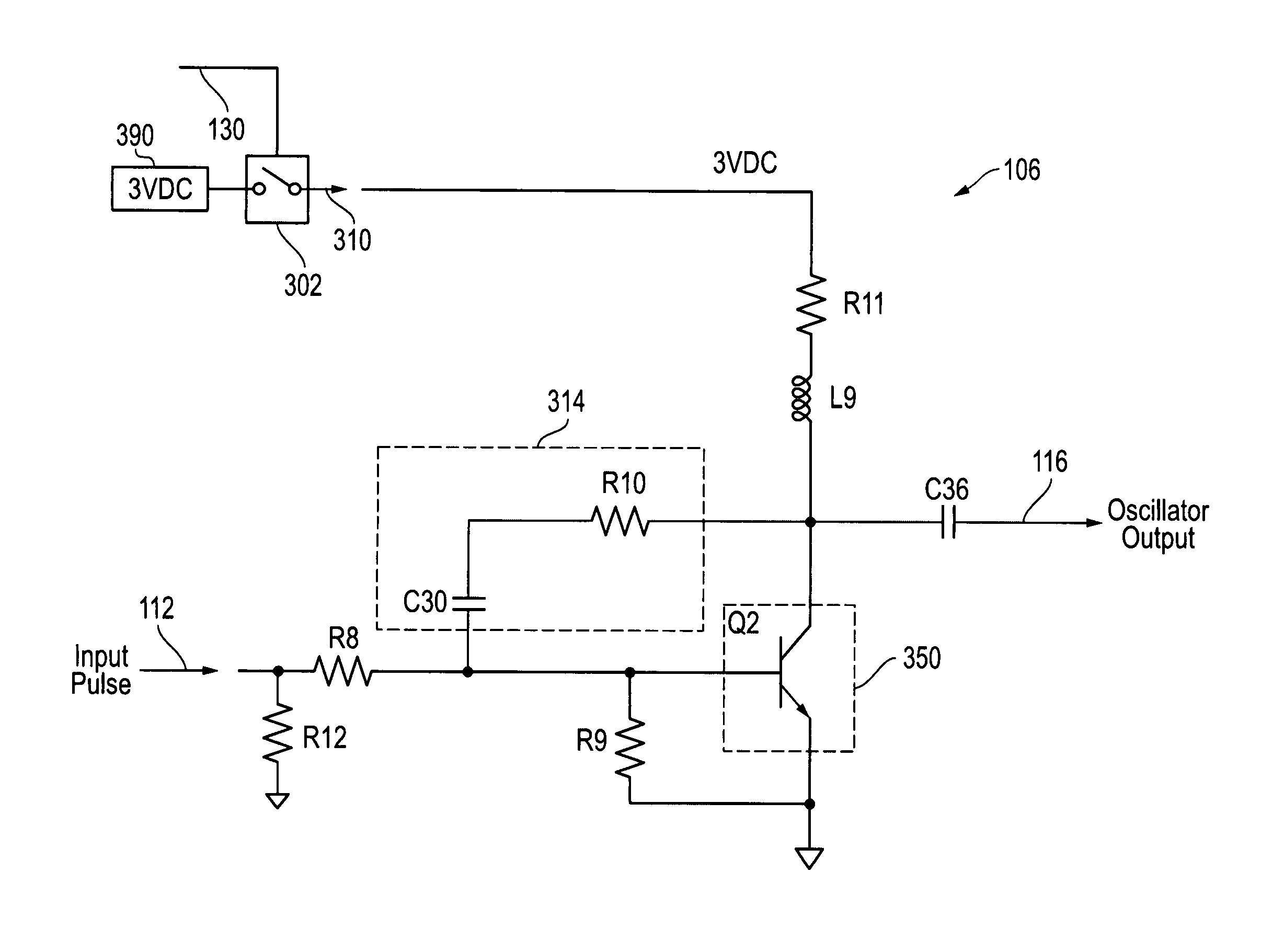
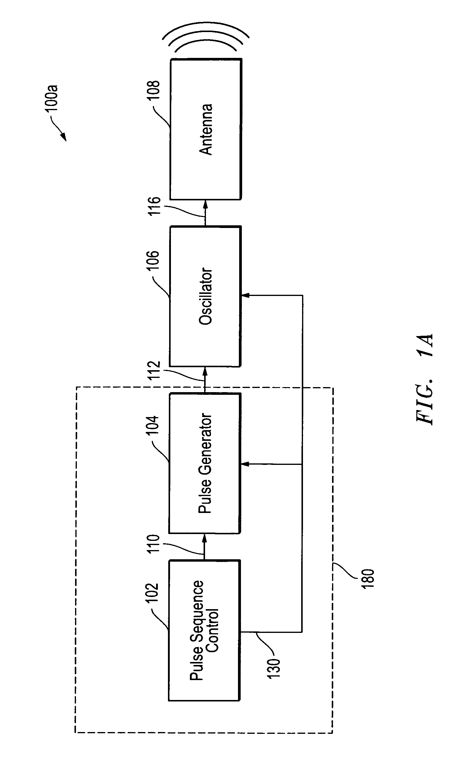
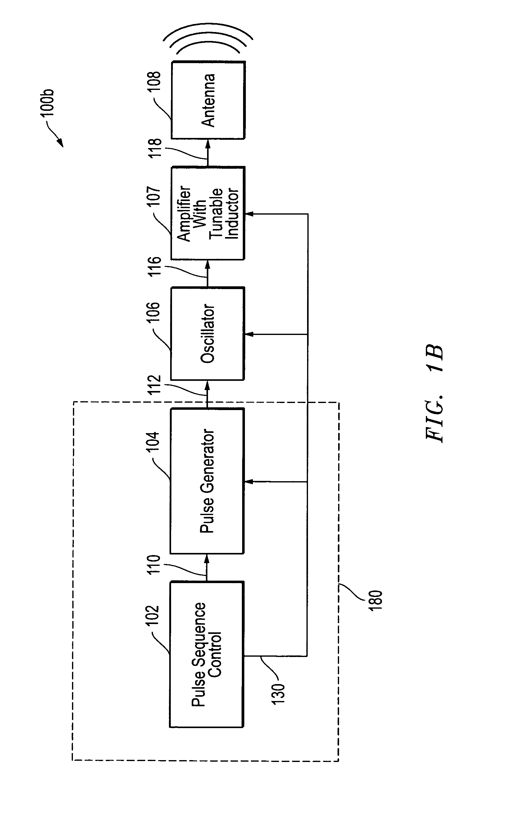
[0017]FIG. 1A illustrates one exemplary embodiment of a RF signal generation system 100 that includes input pulse creation circuitry 180 which is configured to produce and supply a digital oscillator input voltage pulse 112 to a signal input of oscillator circuitry 106, which in turn produces an RF output signal 116 for transmission by antenna 108, e.g., as RF signals in the voltage output to antenna 108 that meet the characteristics defined by the FCC for UWB signals. RF signal generation system 100 may be employed as transmitter circuitry of, for example, a battery-powered portable radio frequency identification (RFID) tag. In this exemplary embodiment, input pulse creation circuitry 180 includes pulse sequence control circuitry 102 and pulse generator circuitry 104 which will be described in further detail herein. However, it will be understood that any other circuitry configuration suitable for producing a digital oscillator input voltage pulse 112 having the characteristics des...


PUM


Abstract

Systems and methods for generating pulsed output signals that employ a gated RF oscillator circuit having an output that is switchably grounded through the emitter of a transistor and including feedback from the output of the circuit to the base of the transistor to create oscillations and to allow a digital input pulse of a desired length to control the start and stop of oscillations created by the transistor.

Description

FIELD OF THE INVENTION[0001]This invention relates generally to signal generation, and more particularly to a gated RF oscillator circuit and use of same for pulsed signal generation.BACKGROUND OF THE INVENTION[0002]As defined by the FCC, an ultra-wideband (UWB) signal is an antenna transmission in the range of 3.1 GHz up to 10.6 GHz at a limited transmit power of −41.3 dBm / MHz with an emitted signal bandwidth that exceeds the lesser of 500 MHz or 20% of the center frequency. UWB signals are currently employed for high-bandwidth, short range communications that use high bandwidth radio energy that is pulsed at specific time instants.[0003]Applications for FCC-defined transmissions include distance-based location and tracking applications, and localization techniques that employ precision time-of-arrival measurements. Examples of such UWB applications include RFID tags that employ UWB communication technology for tracking, localization and transmitting information. Other types of UWB...

Claims


Application Information

Patent Timeline
Patent Type & Authority Patents(United States)
IPC IPC(8): H03C1/62H03C1/02H03B5/20
CPCH03K3/28H03K3/80
Inventor MCCLAIN, JR., ROSS A.RUTHERFORD, BRIAN C.
Owner L 3 COMM INTEGRATED SYST
Why Eureka
Try Eureka