High voltage semiconductor device and driving circuit

a driving circuit and semiconductor technology, applied in the direction of oscillator generators, pulse techniques, electronic switching, etc., can solve the problems of relatively large electric current increase losses, achieve high switching response speed, reduce power loss, and block high voltage

Active Publication Date: 2014-03-18
FUJI ELECTRIC CO LTD
View PDF13 Cites 2 Cited by
  • Summary
  • Abstract
  • Description
  • Claims
  • Application Information

AI Technical Summary

Benefits of technology

[0047]According to the high voltage, semiconductor device and driving device of the invention, a high voltage transistor with a high switching response speed can be provided. Furthermore, a driving circuit with reduced power loss and occurrence of malfunctions can be provided.
[0048]The use of the structure according to the invention, when the area of the circular voltage blocking region, for example, becomes an area that allows to drive a current exceeding the current driving capability required for a high voltage MOSFET to ensure its high voltage blocking capability, enables parasitic capacitance components to be made ineffective in voltage blocking regions other than the region where a current must be driven by required current driving capability. This can reduce the output capacitance of the high voltage MOSFET at a low cost. Therefore, the use of the high voltage MOSFET in a level shift circuit enables a displacement current at an occurrence of a dV / dt surge to be made small.
[0049]Moreover, by reducing an output capacitance of a high voltage MOSFET, when an on-signal is input to the gate of the high voltage MOSFET, the discharge of the output capacitance can be made quickened. Furthermore, when the high voltage MOSFET is used in a level shift circuit, the length of a transmission delay of a signal at turning-on or turning-off in a high electric potential side driving circuit can be shortened. With the transmission delay of a signal thus shortened, the on-duty time in periodic on-off driving of the high voltage MOSFET can be also set to be short to allow the resistance value of a load resistor for level-shifting to also be small. As a result, while power loss in a level shift circuit is reduced, both a displacement current and a load resistance at the occurrence of a dV / dt surge become small, by which the voltage drop in a load resistance section becomes small to enable realization of a driving circuit less susceptible to malfunction due to a dV / dt surge.

Problems solved by technology

However, as shown in the section encompassed by the dotted line in FIG. 13, in the high electric potential side, low voltage circuit section, whose reference electric potential changes, particularly in the case when the reference voltage is high, losses due to the relatively large electric current increase.

Method used


Image

  • High voltage semiconductor device and driving circuit
  • High voltage semiconductor device and driving circuit
  • High voltage semiconductor device and driving circuit

Examples


first embodiment

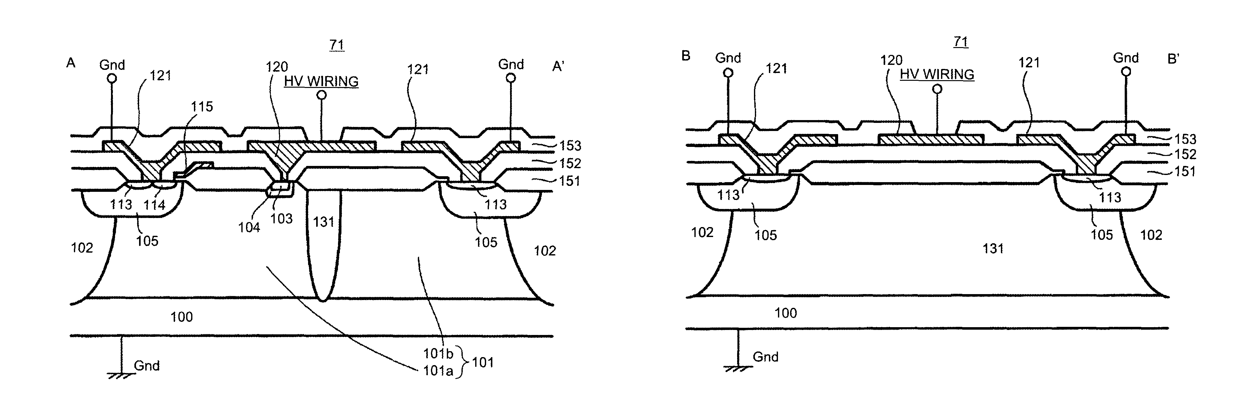
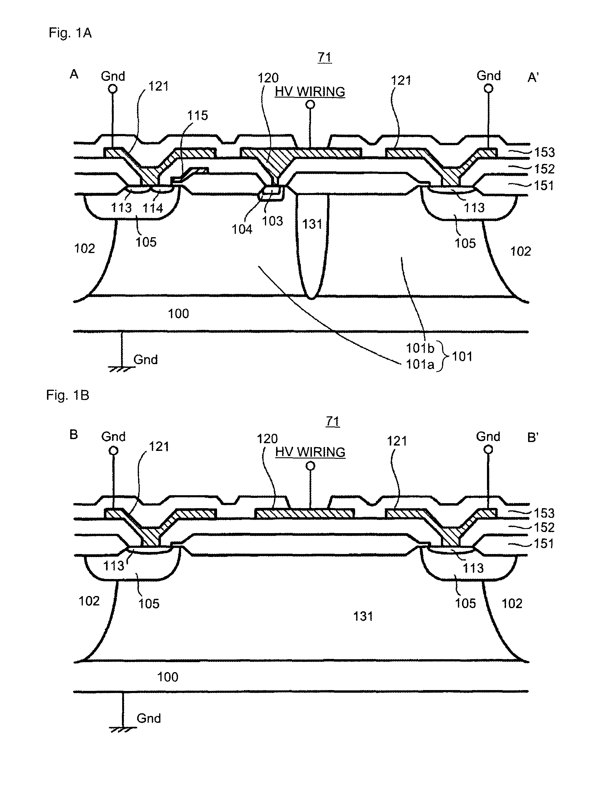
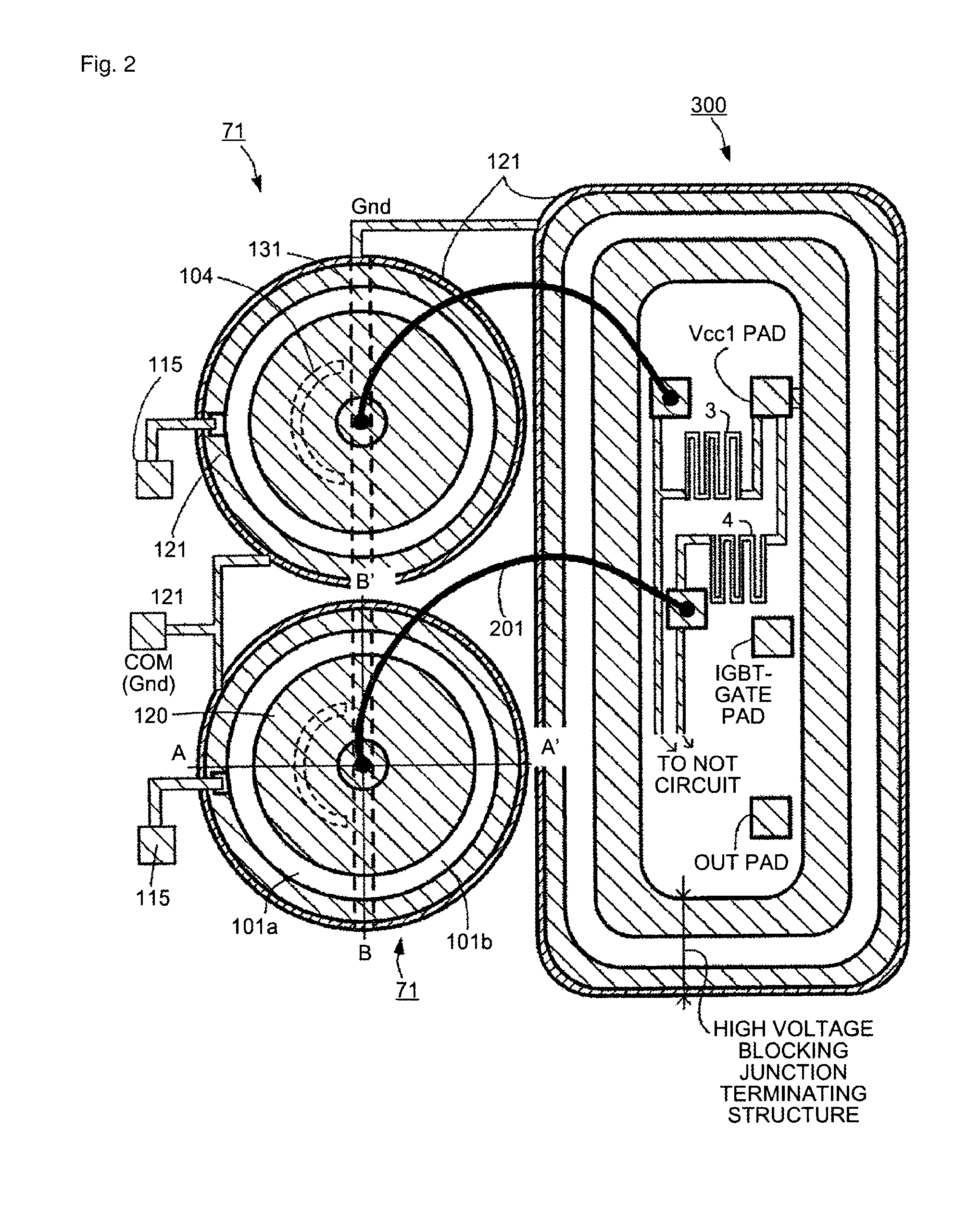
[0080]A first embodiment will be explained with reference to FIG. 1A to FIG. 5, and FIG. 13. FIGS. 1A and 1B are cross sectional views of a principal part of a high voltage MOSFET according to the first embodiment of the invention. FIG. 2 is a plan view of a principal part of a high voltage IC according to the invention. In FIG. 2, a level shift circuit including the high voltage MOSFET and a driving circuit equipped with a floating electric potential region are formed on a single semiconductor substrate (hereinafter, for FIGS. 6 and 9A as well). A cross sectional view taken along line A-A′ in FIG. 2 corresponds to the cross sectional view shown in FIG. 1A and a cross sectional view taken along line B-B′ in FIG. 2 corresponds to the cross sectional view shown in FIG. 1B. In FIG. 2, of semiconductor regions in a high voltage MOSFET 71, only an n offset region 104 and a p−-region 131 are shown by broken lines.

[0081]The high voltage MOSFETs 71 shown in FIGS. 1A and 1B correspond to the...

second embodiment

[0106]FIG. 6 is a plan view showing a principal part of a high voltage IC according to a second embodiment of the invention. A cross sectional view taken along line A-A′ in FIG. 6 is the same as the cross sectional view of the first embodiment shown in FIG. 1A.

[0107]As shown in FIG. 6, a high voltage MOSFET 72 differs from the high voltage MOSFET 71 shown in FIG. 2 in that the plane figure of the p−-region 131 is formed into a V-shape. With the n−-type region 101 divided by the V-shaped p−-region 131 in this way, the area of the section functioning as a MOSFET becomes approximately one-fourth of the area of the corresponding section of the related MOSFET. This can reduce a parasitic output capacitance in the high voltage MOSFET 72 by 60 percent up to a maximum of the order of 75 percent compared with that of the example of a related high voltage MOSFET.

[0108]As explained, according to the second embodiment, the effects of the first embodiment can be achieved.

third embodiment

[0109]FIG. 7 is a plan view showing a principal part of the high voltage MOSFET 73 according to a third embodiment of the invention. A high voltage MOSFET 73 differs from the high voltage MOSFET 72 shown in FIG. 6 in that the n−-type region 101b (a region at a floating electric potential) divided by the p−-region 131 is formed of a plural sections. In this way, the region divided by the p−-region 131 is not necessarily one region but can be formed of a plural regions.

[0110]As explained, according to the third embodiment, the effects of the first embodiment can be achieved.


PUM


Abstract

A high voltage semiconductor device is provided and includes an n−-type region encompassed by a p− well region and is provided on a p−-type silicon substrate. A drain n+-region is connected to a drain electrode. A p base region is formed so as to be separate from and encompass the drain n+-region. A source n+-region is formed in the p base region. Further, a p−-region is provided that passes through the n−-type region to the silicon substrate. The n−-type region is divided, by the p−-region, into a drift n−-type region having the drain n+-region and a floating n−-type region having a floating electric potential.

Description

TECHNICAL FIELD[0001]The present invention relates to a high voltage semiconductor device and driving circuit. In particular, the invention relates to, for example, a control electrode of a controllable semiconductor element such as a semiconductor switching element in an upper arm of an electric power inverting bridge circuit in a PWM inverter or a switching power supply, i.e., a high voltage semiconductor device used as a level shift circuit that is used when a turning-on or -off signal is transmitted without any particular electric potential insulation from a circuit connected to a common electric potential point to the control electrode of a controllable semiconductor device in a circuit in which the electric potential of an electrode (such as an emitter electrode or a source electrode), which is to be the reference for the electric potential of an input driving control signal, changes with respect to a common electric potential such as the ground potential. Furthermore, the inv...

Claims


Application Information

Patent Timeline
Patent Type & Authority Patents(United States)
IPC IPC(8): H03K3/00
CPCH03K2217/0081H01L29/402H01L29/7816H01L29/42368H01L29/4238H01L29/0646H03K17/567H03K17/6871H03K2217/0063H01L29/1095H01L29/41758H01L29/0696H01L2224/05552H01L2224/48091H01L2224/02166H01L2924/13091H01L2924/1301H01L24/05H01L2924/13055H01L2224/04042H01L2924/12036H01L2924/14H01L2224/05555H01L2924/00014H01L2924/00
Inventor YAMAJI, MASAHARU
Owner FUJI ELECTRIC CO LTD
Why Eureka
Try Eureka