Image sensor with double integration time and conditional selection

a technology of image sensor and conditional selection, applied in the field of image sensor, can solve problems such as loss of dynamic range and interval reduction

Active Publication Date: 2014-04-01
TELEDYNE E2V SEMICON SAS
View PDF6 Cites 7 Cited by
  • Summary
  • Abstract
  • Description
  • Claims
  • Application Information

AI Technical Summary

Benefits of technology

[0010]To avoid these drawbacks, the invention proposes to use parts of the analog-digital converter to test the differential voltage between the first and the second sample after these samples have been stored and before the instant scheduled for the third sampling. The analog-digital converter is a ramp-type converter using a linear voltage ramp and a differential amplifier with large gain which toggles when the difference of voltage on its two inputs becomes zero on account of the voltage ramp. According to the invention, a short linear voltage ramp of fixed duration and known slope will be applied; if the amplifier has toggled before the end of the ramp, it will be considered that the illumination has remained below a threshold and a conclusion will be drawn therefrom regarding a new sampling to be done in the first capacitor. The third sampling, when it is performed, replaces the first sample. The definitive analog-digital conversion is done on the samples stored after the instant reserved for the third sampling, whether or not there has been a third sampling.

Problems solved by technology

Firstly a comparator (bulky) is necessary for each column. Then, the test is done on an absolute value of the potential of a column conductor receiving the level of potential of the storage node at the moment of selecting a row of pixels. This potential is compared with a threshold which defines the risk of saturation. The test therefore pertains to an absolute value of level of potential, not to a differential value (useful level of potential minus reinitialization level). This creates an uncertainty in the choice of the threshold to be used. Moreover, there are other uncertainties in the value of the threshold that must be applied to the comparator in order to detect a risk of saturation. These uncertainties are related to variations in the manufacturing method, to temperature variations, to the differences in offset voltage of the reading transistors in the various pixels, to the differences of offset voltages of the comparators corresponding to the various columns of the matrix of pixels. It is therefore mandatory to take significant margins in order to determine the threshold making it possible to know whether or not there is a risk of saturation. This entails a loss of dynamic range, that is to say a reduction in the interval of illuminations that the sensor can actually measure for a given duration of integration. Finally, the necessity to do this voltage comparison at a moment other than the moment of the sampling of a level of potential of the column conductor entails additional current consumption. Indeed, the column conductor is energized only during the phases where it has to copy the level of potential of the storage node. Here, it must be energized both during the test and during the third sampling which is posterior to this comparison.

Method used


Image

  • Image sensor with double integration time and conditional selection
  • Image sensor with double integration time and conditional selection
  • Image sensor with double integration time and conditional selection

Examples


Embodiment Construction

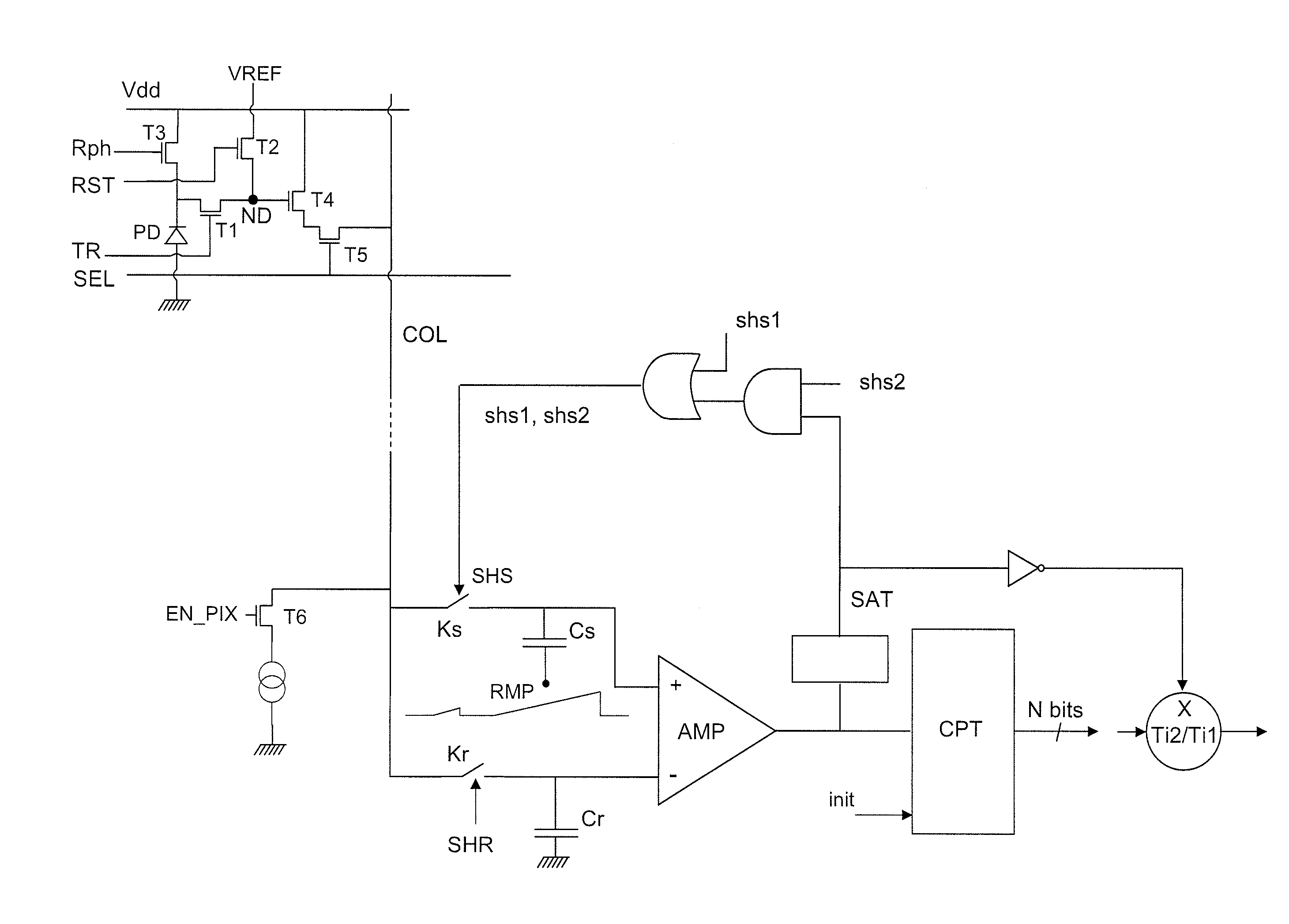
[0024]An active pixel with five transistors and a reading circuit of a sensor according to the invention are represented in FIG. 1. The structure of the pixel is conventional. It comprises a photodiode PD, a capacitive storage node ND (represented by a simple point in FIG. 1, and embodied in practice by an N-type diffusion in a P-type layer), a transistor for charge transfer T1 between the cathode of the photodiode and the storage node, a transistor T2 for reinitializing the potential of the storage node, a transistor T3 for reinitializing the potential of the photodiode, a follower transistor T4, a row selection transistor T5. For a pixel with four transistors the transistor T3 would be dispensed with.

[0025]The transfer transistor T1 is controlled by a transfer signal TR. The transistor T2 has its drain linked to a reference potential VREF and it is controlled by a reinitialization control signal RST. The transistor T3 is linked between the cathode of the photodiode and a reference...


PUM


Abstract

An image sensor for gathering images at one and the same time at low illumination level and at high illumination level is described. The sensor operates with a double integration time at each frame. Two successive charge transfers from a photodiode to a storage node are performed, the first after a first duration, the second after a second duration different from the first. The potential of the storage node after the first transfer of charge is sampled in a first capacitor of the reading circuit. The potential after a reinitialization of the storage node is sampled in a second capacitor. A level of potential taken after the second transfer is conditionally resampled in the first capacitor. The condition of the resampling is a condition of signal level after the first transfer. This level is applied to the differential amplifier of a ramp-type converter for a short duration of ramp.

Description

RELATED APPLICATIONS[0001]The present application is based on, and claims priority from, French Application No. 1152415, filed Mar. 23, 2011, the disclosure of which is hereby incorporated by reference herein in its entiretyFIELD OF THE INVENTION[0002]The invention relates to image sensors, and more particularly to those which are intended to gather images at one and the same time at low luminance level and at high luminance level.BACKGROUND OF THE INVENTION[0003]In general, active pixels comprise a photodiode and three, four or five MOS transistors making it possible to control the reading of the charge generated by light in the photodiode. Pixels with four transistors operate by firstly transferring from the photodiode to a capacitive storage node the charge generated by light, and then by carrying the potential of the storage node over to a column conductor; one of the transistors serves to reinitialize the potential of the storage node before the transfer of charge from the phot...

Claims


Application Information

Patent Timeline
Patent Type & Authority Patents(United States)
IPC IPC(8): H01L27/00
CPCH04N5/35581H04N5/35554H04N5/35536H04N25/58H04N25/583H04N25/589H04N25/00
Inventor NOIRET, ANDYLIGOZAT, THIERRY
Owner TELEDYNE E2V SEMICON SAS
Why Eureka
Try Eureka