Charge controlled avalanche photodiode and method of making the same

a photodiode and avalanche technology, applied in the field of electromagnetic avalanche photodiodes and a method of making the same, can solve the problems of requiring a relatively thick charge control layer, adversely affecting the bandwidth of the device, and reducing the efficiency of the method, so as to prevent the breakdown of the charge carrier, reduce the risk of becoming saturated, and improve the effect of the charge control layer

Inactive Publication Date: 2005-02-10
PICOMETRIX
View PDF17 Cites 17 Cited by
  • Summary
  • Abstract
  • Description
  • Claims
  • Application Information

AI Technical Summary

Benefits of technology

[0003] The APD structure provides the primary benefit of large gain through the action of excited charge carriers that produce large numbers of electron-hole pairs in the multiplication layer. However, an APD is so efficient at producing large numbers of charge carriers that it runs the risk of becoming saturated, thus adversely affecting the bandwidth of the device. In order to prevent charge carrier breakdown, it is imperative that the electric field be regulated within the APD itself, and in particular it is desirable to have the electric field in the multiplication layer be significantly higher than that in the absorption layer.
[0004] Traditionally, a separate absorption, grading, charge, multiplication (SAGCM) APD utilizes a grading layer to minimize hole trapping at the heterojunction interface and a charge control layer to separate the electric field between the absorption and the multiplication layers. Design of this charge control layer is extremely critical in that it should allow for a high enough electric field strength to initiate impact ionization in the multiplication layer while keeping the electric field in the absorption layer low in order to prevent tunneling breakdown.
[0005] For example, an SAGCM APD structure with an n-type multiplication layer, electrons are multiplied and a p-type doping is required to act as the charge control layer. However, a conventional beryllium or zinc p-type doping method requires a relatively thick charge control layer because of the high diffusion coefficient associated with beryllium and zinc. Due to this thick charge control region with lower doping, the carrier transit time across the charge control layer is increased, thereby reducing the overall speed of these APD devices.

Problems solved by technology

However, an APD is so efficient at producing large numbers of charge carriers that it runs the risk of becoming saturated, thus adversely affecting the bandwidth of the device.
However, a conventional beryllium or zinc p-type doping method requires a relatively thick charge control layer because of the high diffusion coefficient associated with beryllium and zinc.
Due to this thick charge control region with lower doping, the carrier transit time across the charge control layer is increased, thereby reducing the overall speed of these APD devices.

Method used


Image

  • Charge controlled avalanche photodiode and method of making the same
  • Charge controlled avalanche photodiode and method of making the same

Examples


Embodiment Construction

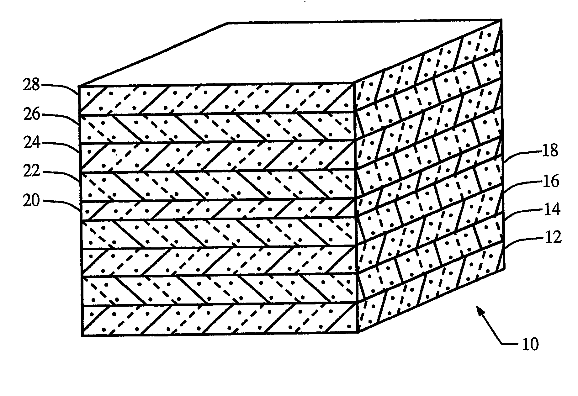
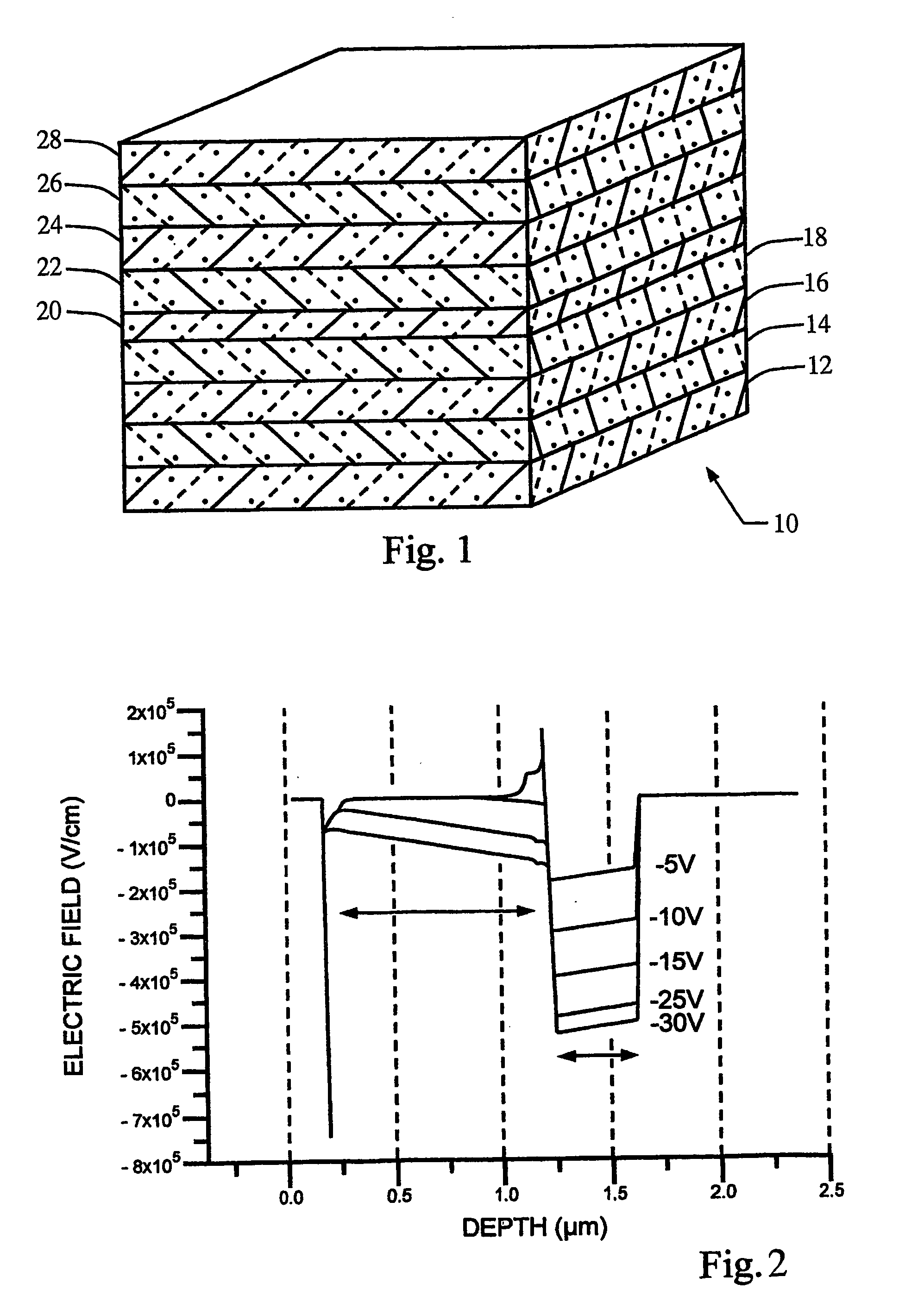
[0010] In accordance with a preferred embodiment of the present invention, an epitaxial structure is provided for photoconductive purposes. The photoconductive structure is an avalanche photodiode (APD) that is optimized for increased performance through a charge control layer. The particulars of the structure and method of manufacture of the present invention are discussed further herein.

[0011] Referring to FIG. 1, a perspective view of a charge controlled APD 10 is shown in accordance with the preferred embodiment. A substrate 12 is provided as a base upon which the epitaxial structure is deposited. The charge controlled APD 10 of the present invention may be manufactured in a number suitable fashions, including molecular beam epitaxy and metal organic vapor phase epitaxy.

[0012] The substrate 12 may be composed of a semi-insulating material or alternatively the substrate may be doped Indium Phosphate (InP). A buffer layer 14 is disposed above the substrate 12 to isolate any stru...


PUM


Abstract

The present invention includes an epitaxial structure (16) grown on a semi-insulating InP substrate (12). First, a buffer layer (14) is grown to isolate defects originated from substrates (12). Then an n-type layer (18) is grown to serve as n-contact layer to collect electrons. Next, a multiplication layer (20) is grown to provide avalanche gain for the APD device (10). Following that, an ultra-thin charge control layer (22) is grown with carbon doping. An absorption layer (24) is grown to serve as the region for creating electronhole pairs due to a photo-excitation. Finally, a p-type layer (28) is grown to serve as p-contact layer to collect holes.

Description

FIELD OF THE INVENTION [0001] The present invention relates generally to the field of semiconductor-based photodetectors, and more specifically to an optimized avalanche photodiode and a method of making the same. BACKGROUND AND SUMMARY OF THE INVENTION [0002] Owing to the known interaction between photons and electrons, great advances have been made in the field of photodetectors in recent years, particularly in those photodetectors that utilize semiconductor materials. One type of semiconductor-based photodetector is termed an avalanche photodiode, or APD. This type of structure is generally composed of a number of solid semiconductive materials that serve different purposes such as absorption and multiplication. [0003] The APD structure provides the primary benefit of large gain through the action of excited charge carriers that produce large numbers of electron-hole pairs in the multiplication layer. However, an APD is so efficient at producing large numbers of charge carriers t...

Claims


Application Information

Patent Timeline
Patent Type & Authority Applications(United States)
IPC IPC(8): H01LH01L21/00H01L21/18H01L31/0304H01L31/0328H01L31/0336H01L31/072H01L31/107H01L31/109H01L47/00
CPCH01L31/03046Y02E10/544H01L31/1075H01L31/107
Inventor KO, CHENG C.
Owner PICOMETRIX
Why Eureka
Try Eureka