

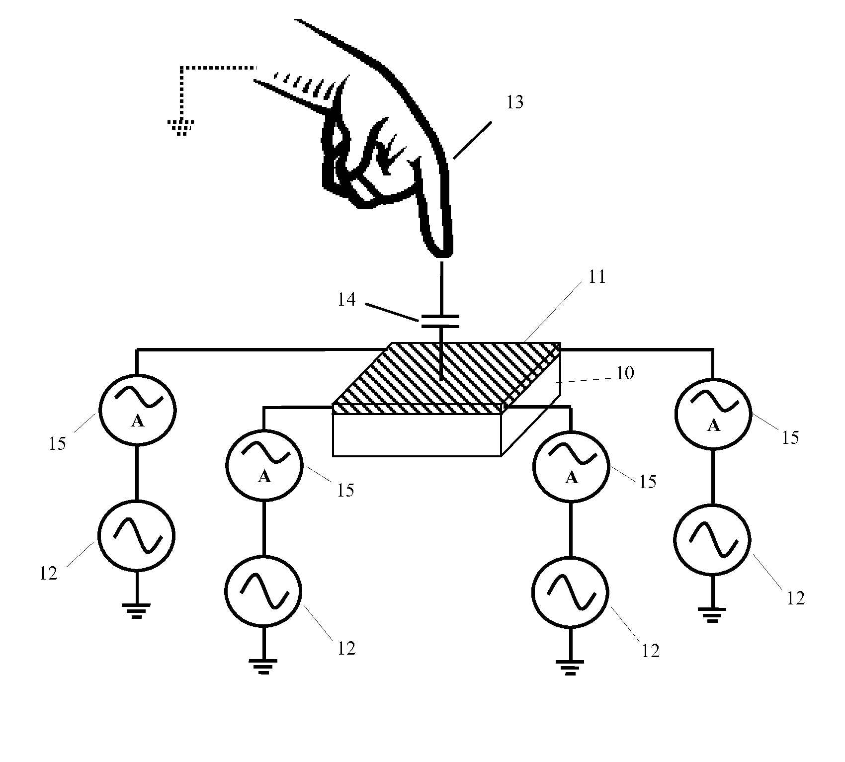
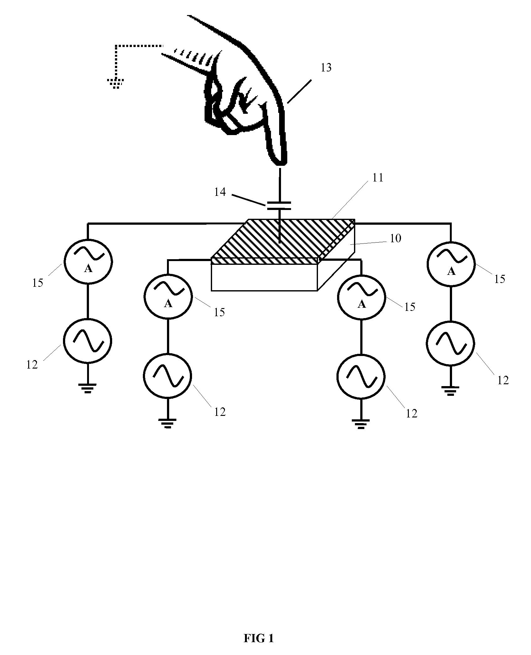
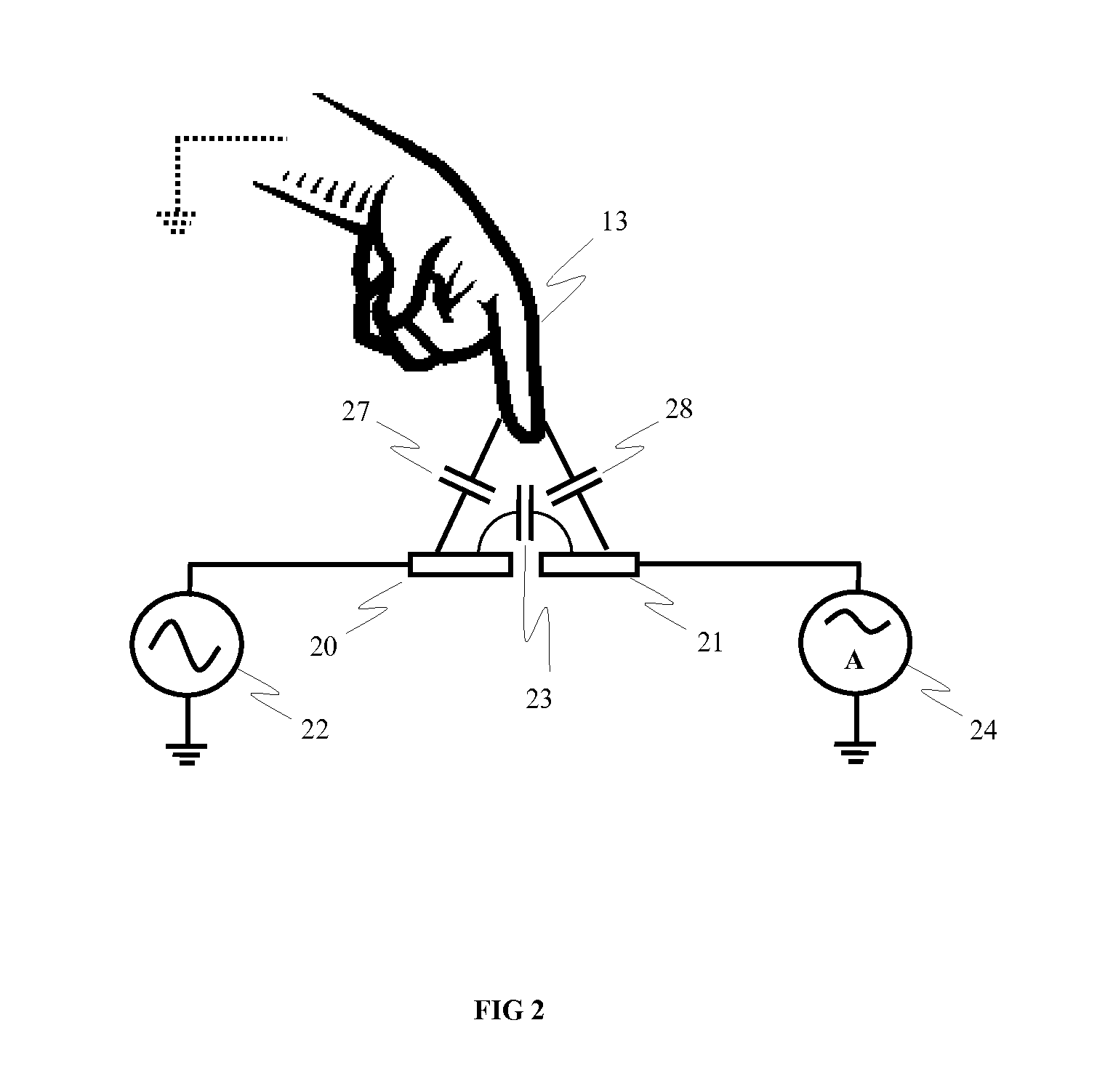
Dual mode capacitive touch panel
a capacitive touch panel and capacitive technology, applied in the field of capacitive touch panel devices, can solve the problems of reducing the accuracy of capacitive touch panel, so as to reduce the sensitivity, spatial resolution and mechanical robustness, the effect of limiting the sensitivity
- Summary
- Abstract
- Description
- Claims
- Application Information
AI Technical Summary
Benefits of technology
Problems solved by technology
Method used
Image

Examples
second embodiment
[0200]In a device in accordance with the present invention, a plurality of connections are made to the shield layer. These connections 1010 could be continuous around the periphery of the shield layer (e.g., a distributed ground connection), as shown in FIG. 11. For certain geometries of sensor, this may yield a more uniform distribution of resistance from each point on the shield layer 920 to the DC voltage source 852. The connections could be made, for example, via conductive glue, or via a conductive metallic track deposited in contact with the shield layer material. Since every point on the shield layer exhibits a similar resistance RG 855 to the DC voltage source 852, an advantage of this embodiment is that each intersection in the array generates a similar response to a certain input stimulus.
third embodiment
[0201]In a device in accordance with the present invention, a grid of conductive tracks 1110 is deposited in contact with the shield layer 920, as shown in FIG. 12 (e.g., the shield includes a grid of conductors that distribute the ground connection). The conductive tracks have a significantly lower sheet resistance than the shield layer material itself, and may be formed from a metal such as aluminium, or from a transparent conductor such as indium tin oxide (ITO). The grid of conductive tracks may provide a superior uniformity of the resistance 855 from each point on the shield layer 920 to the DC voltage source 852. This is advantageous because it ensures that each intersection in the array generates a similar response to a certain input stimulus.
[0202]A fourth embodiment of a device in accordance with the present invention is shown in FIG. 13. The fourth embodiment incorporates a layer of transparent and non-conductive fluid 1210 between the sensor substrate 605 and the shield l...
fifth embodiment
[0203]In a device in accordance with the present invention, the pattern of the drive electrodes 710 and the sense electrodes 720 is optimised in order to improve the signal to noise ratio, compared to that of the simple grid shown in FIG. 6. One possibility is to employ a diamond pattern, for example as disclosed in U.S. Pat. No. 5,543,588 and shown in FIG. 14. Such patterns are well known in the field of projected capacitive touch sensors, and may offer a reduced fringing capacitance 828 between parallel drive electrodes 710 and between parallel sense electrodes 720. This reduced fringing capacitance may improve the signal to noise ratio of the sensor.
[0204]The sheet resistance of the shield layer dictates the resistance RG of the resistive path 855, from a given point on the shield layer to the DC voltage source connection 850. This resistance, together with the size of the various capacitances that form to the shield layer, such as CC2820, CC1825, determines the ‘transition frequ...
PUM
 Abstract
Description
Claims
Application Information