Printed circuit board element and method for the production thereof

a printed circuit board element and printed circuit board technology, applied in the direction of printed circuit elements, instruments, electrical equipment, etc., to achieve the effect of high data transfer rate, high integration of optical signal connections, and highly flexible bending region of printed circuit board elements

Active Publication Date: 2014-04-22
AT & S AUSTRIA TECH & SYSTTECHN AG
View PDF12 Cites 2 Cited by
  • Summary
  • Abstract
  • Description
  • Claims
  • Application Information

AI Technical Summary

Benefits of technology

[0021]The present technology utilizes the advantages of the rigid-flexible printed circuit board and of the TPA structuring of optical waveguides for producing highly-integrated optical signal connections in a printed circuit board element. By means of the proposed technology, it is possible in this case that both optical material, which as a rule is comparatively expensive, is saved and a very thin and consequently highly flexible bending region of the printed circuit board element is realized.
[0022]The present technology may be employed in optoelectronic hybrid printed circuit boards with multi-mode or single-mode wave guides for high data transfer rates, with a gr

Problems solved by technology

Above all, there is also the problem in this case of not negatively affecting the flexibility of the composite printed circuit board elem

Method used


Image

  • Printed circuit board element and method for the production thereof
  • Printed circuit board element and method for the production thereof
  • Printed circuit board element and method for the production thereof

Examples


Embodiment Construction

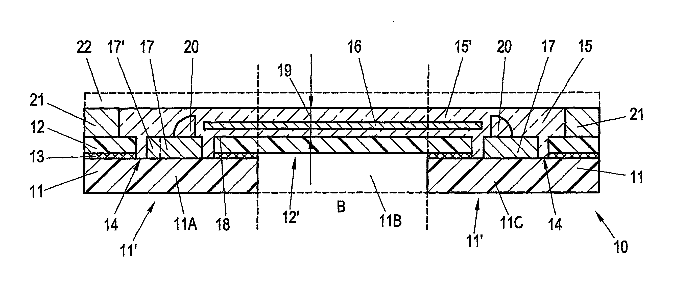
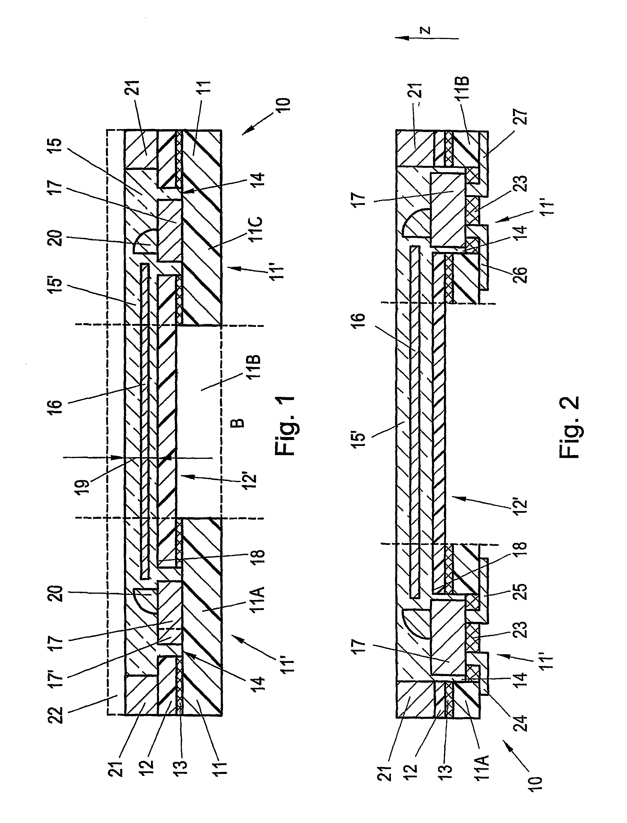
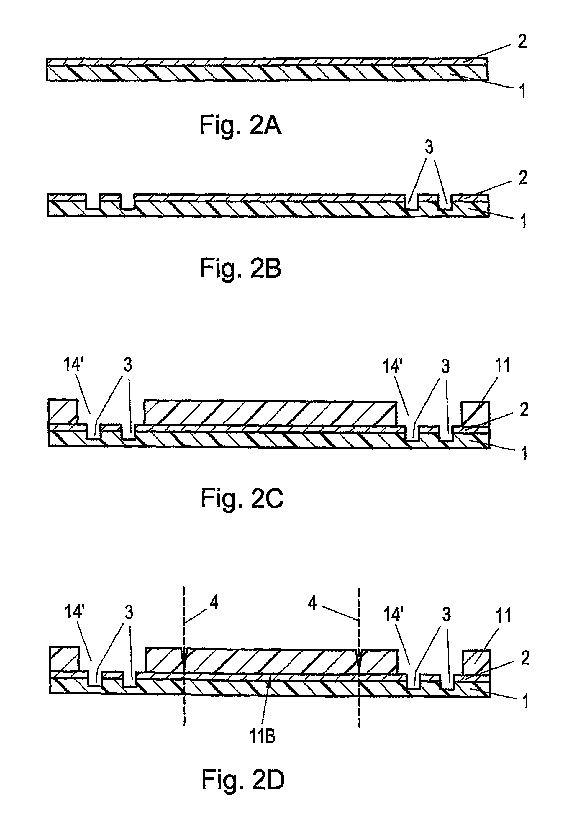
[0032]In FIG. 1, a rigid-flexible printed circuit board 10 is only quite schematically shown, without a true-to-scale illustration of the individual components, which printed circuit board has a rigid substrate 11 as a base, from which two rigid printed circuit board parts (portions) 11A, 11C are formed; these rigid printed circuit board parts 11A, 11C define two rigid areas 11′ and are separated from each other by an open region B which has been obtained by removing a substrate portion 11B indicated in broken lines, and which is bridged by a flexible printed circuit board part (portion) 12 that provides a bendable connection between the two rigid printed circuit board parts 11A and 11C.

[0033]In the exemplary embodiment shown, a separate flexible printed circuit board part 12, e.g. a polyimide film, is provided, which is attached onto the two rigid printed circuit board parts 11A and 11C with the aid of an adhesive layer 13.

[0034]When producing this so-far described rigid-flexible p...


PUM

PropertyMeasurementUnit
Flexibilityaaaaaaaaaa

Abstract

The invention relates to a printed circuit board element (10), comprising at least one flexible printed circuit board part (12) and at least one rigid printed circuit board part (11A, 11C; 34, 35; 37) having a component (17), which is accommodated in a cavity (14) and with a light-emitting or light-receiving part (17) projects over the edge (18) of the cavity (14), wherein the flexible printed circuit board part (12) has a flexible layer (15′) made of an optical, photo-polymerizable material (15), in which an optical fiber (15) is structured in alignment with the light-emitting or light-receiving part (17) of the optoelectronic component (17) by way of radiation.

Description

FIELD OF THE INVENTION[0001]The invention relates to a printed circuit board element with at least one flexible printed circuit board portion and with at least one rigid printed circuit board portion with a component; furthermore, the invention relates to a method of producing such a printed circuit board element.BACKGROUND OF THE INVENTION[0002]Printed circuit board elements with rigid and flexible printed circuit board portions were proposed with regard to the necessity of foldable and bendable connections for the most varying of applications, starting from applications for the mounting of LEDs in steps, cf. e.g. DE 199 09 399 C1, up to applications of such partially flexible printed circuit boards in electronic devices with a foldable portion, such as mobile telephony devices, yet also portable computers (laptops, notebooks) and so-called handhelds, where, beyond hinge joints, a corresponding flexibility was required with regard to data and signal connections, respectively. Besid...

Claims


Application Information

Patent Timeline
IPC IPC(8): G02B6/12
CPCH05K2201/09127G02B6/43G02B6/138H05K3/4691G02B6/4214H05K1/0274Y10T29/49124
Inventor LANGER, GREGORSTAHR, JOHANNES
Owner AT & S AUSTRIA TECH & SYSTTECHN AG
Why Eureka
Try Eureka