Electrostatic movable micro mirror chip

a micro-mirror chip and electrostatic technology, applied in piezoelectric/electrostrictive/magnetostrictive devices, instruments, optics, etc., can solve the problems of high manufacturing cost, difficult to reduce, and inability to provide precise positioning of solder joints, etc., to reduce manufacturing costs, save time, and signal connection

Inactive Publication Date: 2005-09-27
IND TECH RES INST
View PDF8 Cites 2 Cited by
  • Summary
  • Abstract
  • Description
  • Claims
  • Application Information

AI Technical Summary

Benefits of technology

[0008]Both sides of the mirror are coated with metallic layers for good reflection, interconnection and stress-balance for preventing it from deformation. The electrostatic movable micro mirror chip of the invention utilizes fitting solder and positioning grooves for both positioning and jointing. It reduces manufacturing cost and saves time. The signal connection area is prevented from solder stain by means of a shrinking pipe or a stopping wall located between the fitting solder and the signal connection area. The mirror is both-side coated for eliminating any stress generated by construction, material and temperature process and enhancing flatness of the mirror.

Problems solved by technology

In the optical communication industry, requirements of optical components are getting more and more severe.
The biggest challenge in fabrication of a conventional movable micro mirror chip is the positioning alignment of the mirror layer and the actuation layer.
The alignment process requires operations of hands or specific positioning machines that cause a high manufacturing cost very difficult to be reduced.
Though the construction solves conduction and jointing problem, the solder joint does not provide precise positioning.
However, when the solder melts, it loses its form.
In order to stabilize the jointing and to remove the spacer after soldering, special materials for the spacer is required that makes the material selection very difficult.
Also, the height of the solder layers is hard to be controlled after the large temperature variation.
Moreover, since the mirror layer and the actuation layer all require electrical circuit to operate, there are wire-bonding areas on the layers that are easy to be stained by re-flow solder because there is no protection manner.
The melted solder may stain the bonding areas and make the afterward wire bonding impossible, or even ruin the whole chip and increase fabrication cost of the product.

Method used


Image

  • Electrostatic movable micro mirror chip
  • Electrostatic movable micro mirror chip
  • Electrostatic movable micro mirror chip

Examples


Embodiment Construction

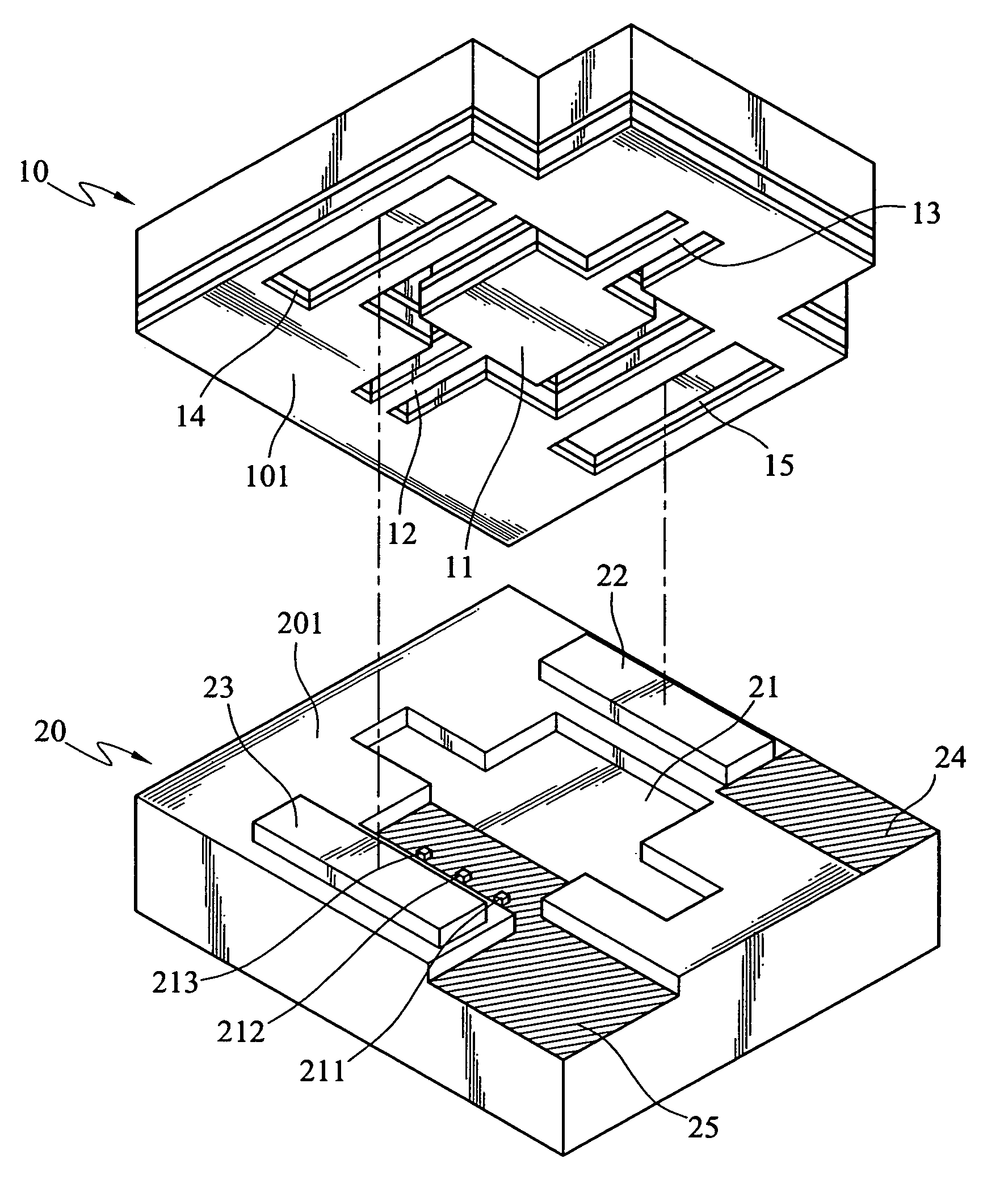
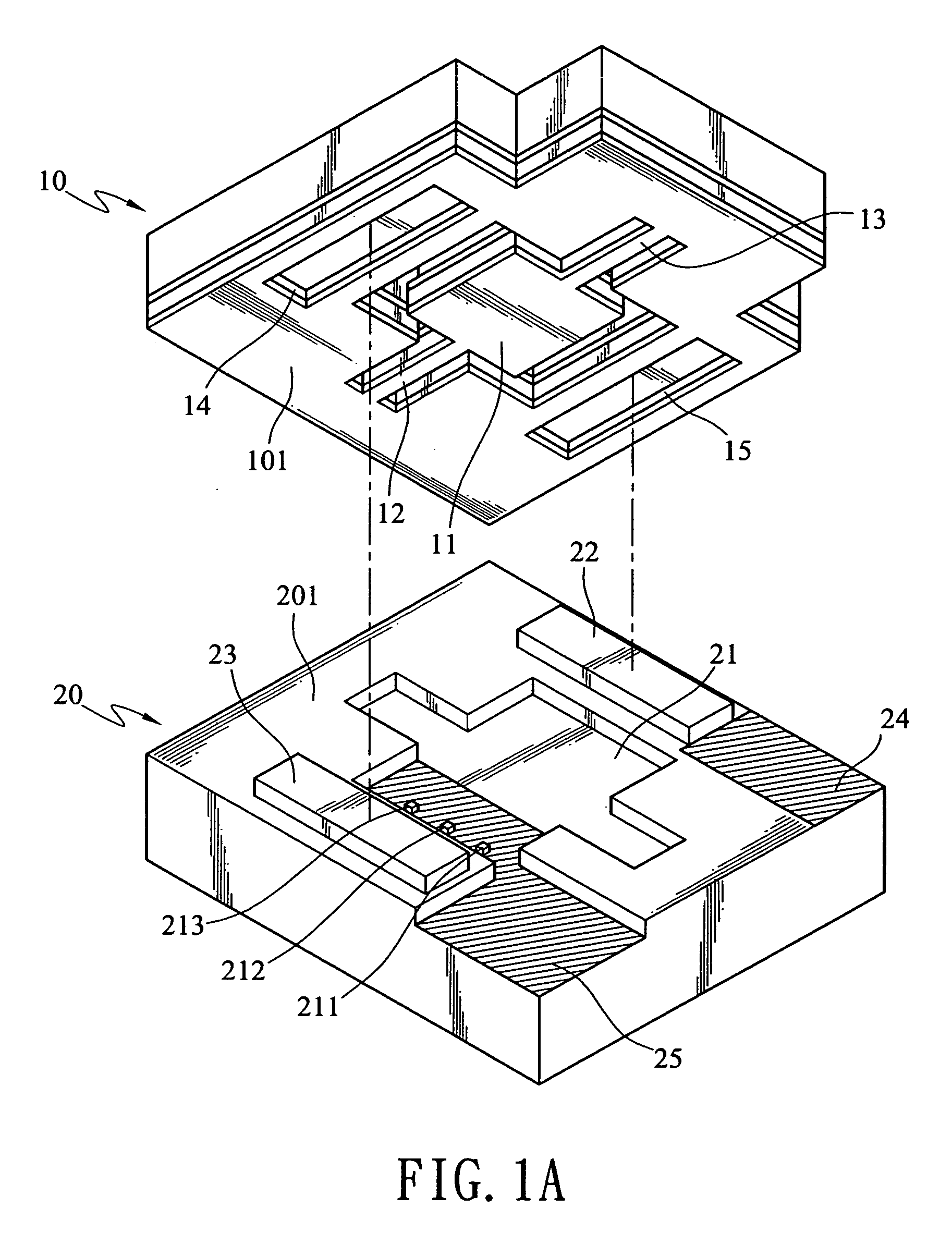
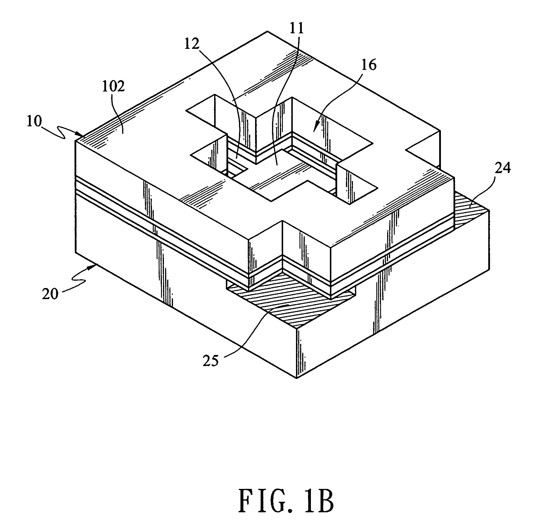
[0020]As shown in FIGS. 1A and 1B, an electrostatic movable micro mirror chip according to the invention includes an upper mirror plate 10 and a lower electrode plate 20. The middle portion of the upper mirror plate 10 carries a mirror 11 that is supported by two arms 12, 13 for revolutions relative to the upper mirror plate 10. The upper mirror plate 10 has a top surface 102 and a bottom surface 101. The top surface 102 is formed with a cavity 16, 21 corresponding to the mirror 11. The mirror 11 has a reflective surface facing up. The top surface 102 is formed with two positioning grooves 14, 15 located preferably on both sides of the mirror 11.

[0021]The lower electrode plate 20 has its top surface 201 jointed with the bottom surface 101 of the upper mirror plate 10. The top surface 210, corresponding to the mirror 11, is formed with a cavity 16, 21 for the mirror 11 freely moving therein. Both sides of the cavity 16, 21, corresponding to the positioning grooves 14, 15, are formed ...


PUM


Abstract

An electrostatic movable micro mirror chip includes an upper mirror plate and a lower electrode plate positioned and jointed together via pairs of fitting solder and positioning grooves. It improves the optical quality of the mirror chip by a lower joining temperature. The fitting and jointing achieves easy positioning and interconnection. The fabrication time and cost is less. The mirror in the mirror chip is plated with metallic coating on both sides so as to balance the stress and improve its flatness.

Description

FIELD OF THE INVENTION[0001]The invention generally relates to an electrostatic movable micro mirror chip applicable to optical communication or optical display industry, and in particular relates to an electrostatic movable micro mirror chip in which solder is used for positioning and jointing.BACKGROUND OF THE INVENTION[0002]In the optical communication industry, requirements of optical components are getting more and more severe. The optical devices suppliers have to provide smaller while cheaper components to meet customer's requirements. By applying semiconductor manufacturing process and other machining processes, kinds of high-precision and high-quality micro mechanical elements can be made in a mass production scale.[0003]Movable micro mirror chip is a kind of micro component applicable in optical communication or display modules. The micro mirror chip mainly includes a mirror layer and an actuation layer. The mirror layer is a suspended mirror actuated to swing or revolve b...

Claims


Application Information

Patent Timeline
Patent Type & Authority Patents(United States)
IPC IPC(8): G02B26/00B81B3/00G02B26/08
CPCG02B26/0841
Inventor CHEN, BING-RUKUO, WU-CHENGCHEN, MING-HUNGWENG, JUI-PINGSU, YEH-ILEE, HSIAO-WEN
Owner IND TECH RES INST
Why Eureka
Try Eureka