Area reduction for surface mount package chips

a technology of active circuit chips and package chips, which is applied in the manufacture of printed circuits, solid-state devices, basic electric elements, etc., can solve the problems of circuits designed for performance that have conflicting requirements, circuits designed for performance and high-sensitive circuit components are not designed to survive esd attacks. , to achieve the effect of reducing the area of surface mount package chips, cost-effective, and reducing parasitic inductan

Inactive Publication Date: 2014-04-29
SHAU JENG JYE
View PDF11 Cites 9 Cited by
  • Summary
  • Abstract
  • Description
  • Claims
  • Application Information

AI Technical Summary

Benefits of technology

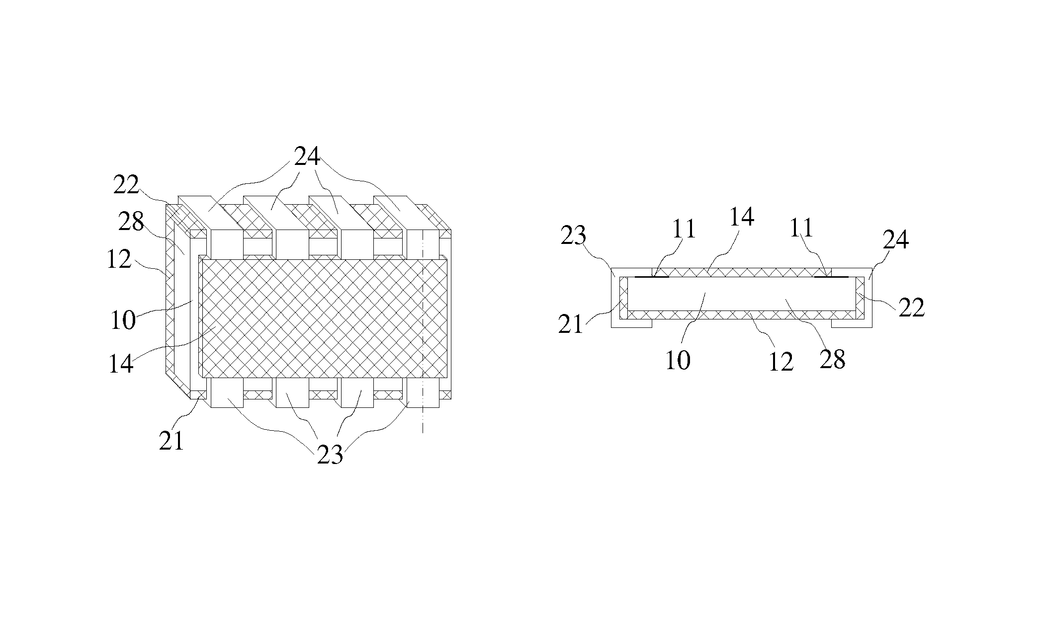
[0025]The primary objective of our preferred embodiment is, therefore, to reduce the area of surface mount package chips that comprise active electrical devices built on silicon substrate(s). The other objective of our preferred embodiment is to provide cost effective surface mount package chips. The other objective of our preferred embodiment is to reduce the parasitic inductance on the I / O connections of surface mount package chips. These and other objectives are achieved by using side-wall conductor leads instead of bumping methods.

Problems solved by technology

ESD is a serious issue in solid state electronics, such as integrated circuits (IC).
Such high sensitive circuit components are not designed to survive ESD attacks.
Circuits designed to survive ESD attacks and circuits designed for performance have conflicting requirements.
The super-fine precision of advanced IC technology makes ESD protection more difficult.
For example, the nano-meter contacts and vias used in advanced IC technologies often become the weak spots during ESD attacks.
Therefore, on-chip ESD protection circuits occupy significant areas, require additional manufacture steps, and cause performance problems.
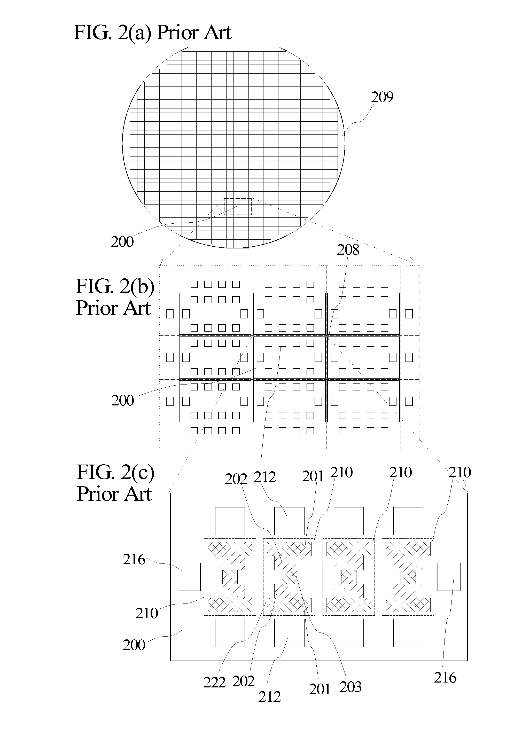
However, the ESD protection circuit on the semiconductor die (200) in FIG. 2(c) is not ready for application; it needs conductor leads to allow board level electrical connections to the electrical components on the die.
Although prior art ESD protection chips have been proven to be highly effective against ESD attacks, their usage is limited.
The most important reason is the area of prior art ESD chips are too large.
There is typically not enough room to place such prior art external ESD chips to protect a large number of signals.
The bonding wires and the lead frames in the integrated circuit packages typically introduce parasitic inductance around 2 nh and parasitic capacitance around 2 pf—values that are large enough to cause problems for high performance signals.
BGA packages are typically smaller than TDFN packages, but the cost of BGA packages are typically higher than TDFN packages of the same I / O count.
The above examples show that formation of conductor leads is the major source of area, cost, and performance problems for prior art external ESD protection chips or electrical diode chips.
Such complex conductor leads on integrated circuit packages typically result in large size, high cost, and high parasitic impedance.
Such resolution is certainly not enough to support the manufacture of advanced integrated circuits, but it is enough to pattern conductor leads of external ESD protection chips or rectifying diodes.

Method used


Image

  • Area reduction for surface mount package chips
  • Area reduction for surface mount package chips
  • Area reduction for surface mount package chips

Examples


Embodiment Construction

[0025]The primary objective of our preferred embodiment is, therefore, to reduce the area of surface mount package chips that comprise active electrical devices built on silicon substrate(s). The other objective of our preferred embodiment is to provide cost effective surface mount package chips. The other objective of our preferred embodiment is to reduce the parasitic inductance on the I / O connections of surface mount package chips. These and other objectives are achieved by using side-wall conductor leads instead of bumping methods.

[0026]While the novel features of the invention are set forth with particularly in the appended claims, our preferred embodiments, both as to organization and content, will be better understood and appreciated, along with other objects and features thereof, from the following detailed description taken in conjunction with the drawing.

BRIEF DESCRIPTION OF THE DRAWINGS

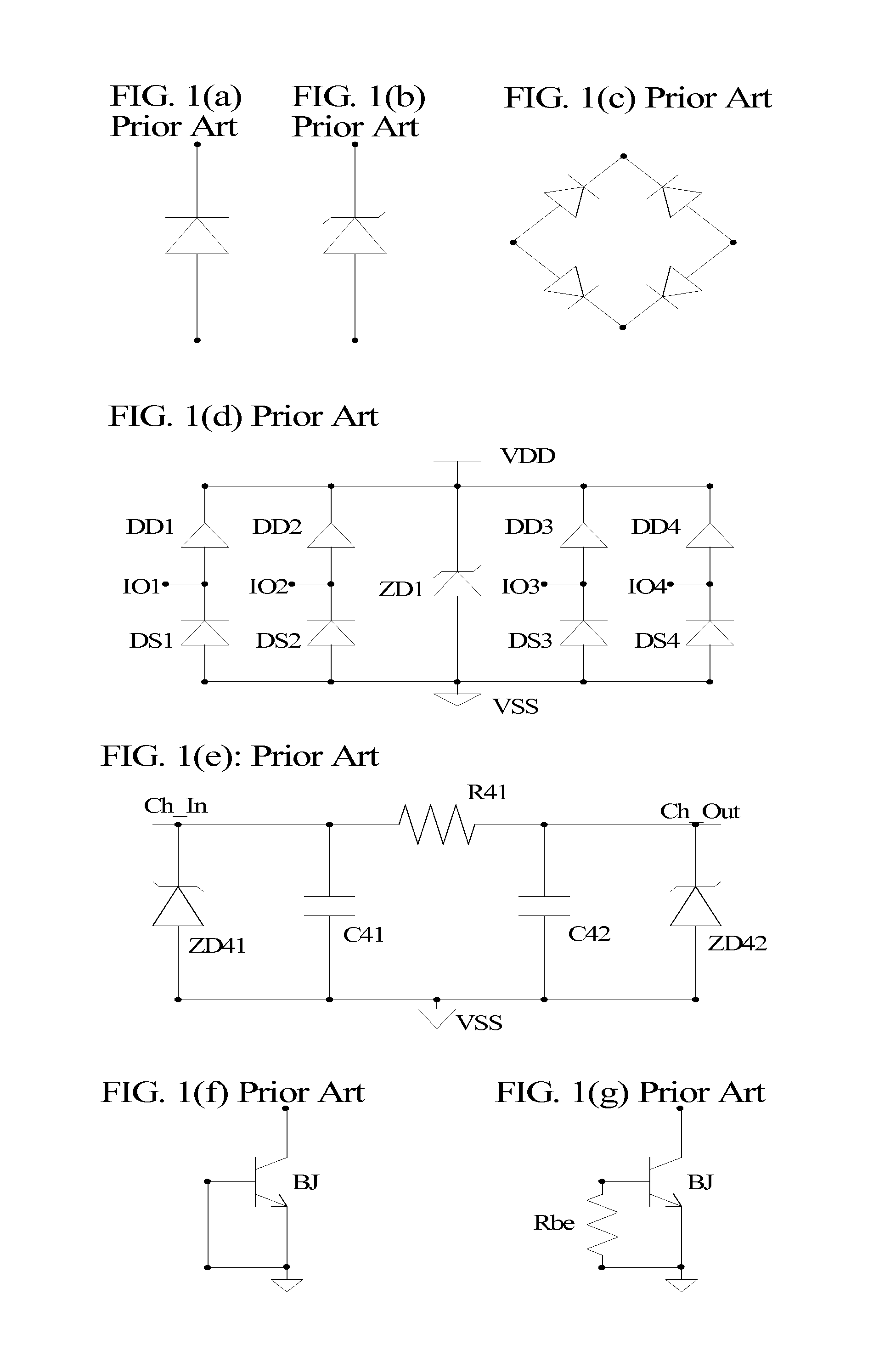
[0027]FIGS. 1(a-g) are schematic diagrams of electrical diodes and ESD protection circu...


PUM

PropertyMeasurementUnit
thicknessaaaaaaaaaa
widthaaaaaaaaaa
widthaaaaaaaaaa

Abstract

Using side-wall conductor leads insulated by side-wall insulators to form package level conductor leads for active circuits manufactured on silicon substrate, the preferred embodiments of the present invention significantly reduces the areas of surface mount package chips. Besides area reduction, these methods also provide significant cost saving and reduction in parasitic impedance.

Description

[0001]This application is a continuation-in-part application of previous patent application with a Ser. No. 12 / 636,474, with a title “Area Reduction for Die-scale Surface Mount Package Chips”, and filed by the applicant of this invention on Dec. 11, 2009. The patent application Ser. No. 12 / 636,474 is a continuation-in-part application of previous patent application with a Ser. No. 12 / 589,163, with a title “Area Reduction for Electrical Diode Chips”, and filed by the applicant of this invention on Oct. 19, 2009.BACKGROUND OF THE INVENTION[0002]The present invention relates to packaging for active circuits, and more particularly to area reduction methods for surface mount packaged active circuit chips.[0003]Semiconductor electrical diodes are commonly used for rectifying circuits and for electrostatic discharge (ESD) protections. By definition, an electrical diode is a two-terminal rectifying semiconductor device used for rectifying or for ESD protection. Examples of electrical diodes...

Claims


Application Information

Patent Timeline
Patent Type & Authority Patents(United States)
IPC IPC(8): H01L23/48H01R43/00
CPCH01L2924/01019H01L2924/00H01L2224/48257H01L2924/19041H01L2924/10253H01L2224/48472H01L2224/16H01L27/0255H01L23/49816H01L2924/01046H01L21/561H01L2224/48091H01L2224/49171H01L2924/14H01L24/48H01L2224/48247H01L24/49H01L21/568H01L25/0657H01L2924/3011H01L25/072H01L2924/00014H01L23/3114H01L2225/06551H01L2924/09701H01L2924/30107H01L2924/15311H01L23/49827H01L2924/12032H01L2924/1305Y10T29/49121Y10T29/49147H01L2924/181H01L2224/05554H01L2924/00012H01L2224/45099H01L2224/45015H01L2924/207H01L23/48
Inventor SHAU, JENG-JYE
Owner SHAU JENG JYE
Why Eureka
Try Eureka