IR(voltage) drop analysis in integrated circuit timing

a technology of integrated circuit and voltage drop, which is applied in the field of measuring ir drop, can solve the problems of overly optimistic static peak ir flow, too many cells, and failure to operate properly when fabricated, so as to reduce power parasitic impedance, improve power supply grid, and increase design effort

Inactive Publication Date: 2014-04-29
APPLE INC
View PDF9 Cites 7 Cited by
  • Summary
  • Abstract
  • Description
  • Claims
  • Application Information

AI Technical Summary

Problems solved by technology

One of the challenges with standard cells is the correct determination of delay in the cells under various operating conditions.
If the maximum delay parameter were shorter than the actual delay, the block would appear to meet timing during the design but would fail to operate properly when fabricated.
This approach is too pessimistic in many cells.
For example, in complex or multiple stage cells, static peak IR flow is overly pessimistic because timing differences between stages are not taken into account.
If the difference in the timing parameters exceeds the margin, additional design effort may be warranted.

Method used


Image

  • IR(voltage) drop analysis in integrated circuit timing
  • IR(voltage) drop analysis in integrated circuit timing
  • IR(voltage) drop analysis in integrated circuit timing

Examples


Embodiment Construction

Overview of Standard Cell Circuits

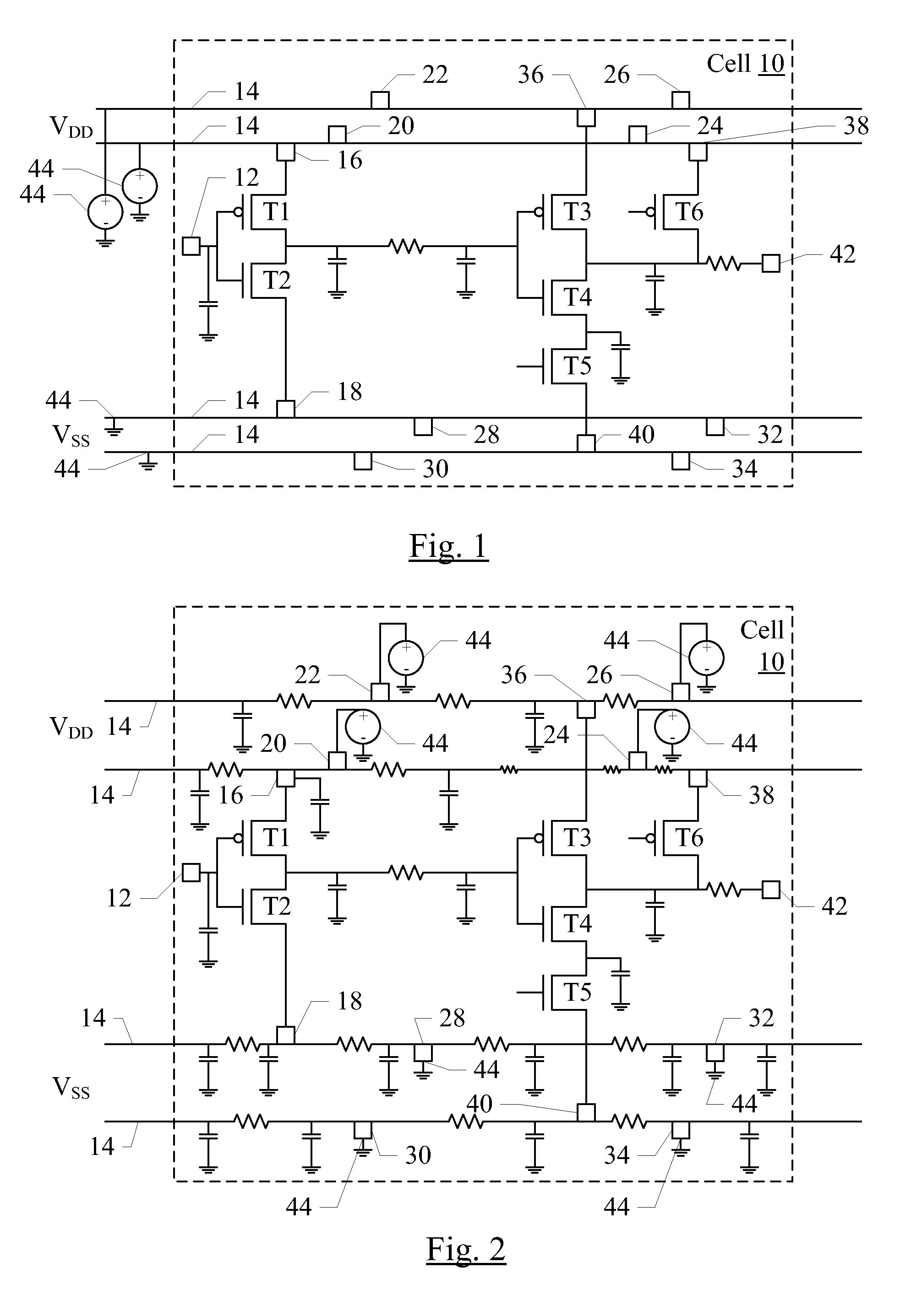
[0017]Turning now to FIGS. 1 and 2, an exemplary standard cell circuit 10 that excludes power parasitic impedances (FIG. 1) and that includes the power parasitic impedances (FIG. 2) are shown. The exemplary cell 10 is merely one embodiment, and numerous other embodiments of standard cell circuits may be used. The cell 10 may be one standard cell defined in a library of standard cells, for example.

[0018]As shown in FIG. 1, the cell 10 includes various transistors T1 to T6. The transistors T1, T3, and T6 are p-type metal-oxide-semiconductor (PMOS) transistors and the transistors T2, T4, and T5 are n-type MOS (NMOS) transistors. The transistors T1 and T2 form an inverter coupled between the power supplies VDD and VSS (e.g. power and ground). The transistors T1 and T2 have gate terminals connected to an input to the cell 10. The connection point for the input is illustrated as a via 12 which may provide connection between the gate terminals (e.g. at a p...


PUM


Abstract

In one embodiment, an IR drop analysis methodology may include characterizing standard cells without including power parasitic impedances, extracting the power parasitic impedances for the standard cells, and characterizing the standard cells with the power parasitic impedances. A set of timing parameters (such as minimum delays and maximum delays through the cells) may be generated from each characterization. The methodology may include comparing the timing parameters from each characterization, and identifying cells for which additional design effort should be expended to improve the power supply grid (e.g. to reduce the power parasitic impedances). For example, a margin may be budgeted for speed loss (delay increase) due to IR drop. If the difference in the timing parameters exceeds the margin, additional design effort may be warranted.

Description

BACKGROUND[0001]1. Field of the Invention[0002]This invention is related to the field of timing methodologies for integrated circuit development and, more particularly, to measuring IR drop on power supply interconnect.[0003]2. Description of the Related Art[0004]The design of an integrated circuit, from concept to “tape out” (i.e. the transmission of the data describing the integrated circuit to the fabrication foundry), is a complex series of parallel, interdependent processes such as logic design, circuit design, synthesis, timing analysis, place and route, verification, etc. To successfully fabricate an integrated circuit that performs as specified, all of the various processes must be completed as accurately as possible.[0005]Many integrated circuit design methodologies rely on synthesis using “standard cell” circuits for significant portions of the design. A standard cell may be a predesigned circuit (including layout and interconnection of the transistors used to form the cir...

Claims


Application Information

Patent Timeline
Patent Type & Authority Patents(United States)
IPC IPC(8): G06G7/54G06F17/50
CPCG06F2217/84G06F17/5031G06F2217/78G06F17/5036G06F30/3312G06F2119/06G06F2119/12G06F30/367
Inventor LAU, BETTY Y.KLASS, EDGARDO F.MEHTA, ANUP S.
Owner APPLE INC
Why Eureka
Try Eureka