

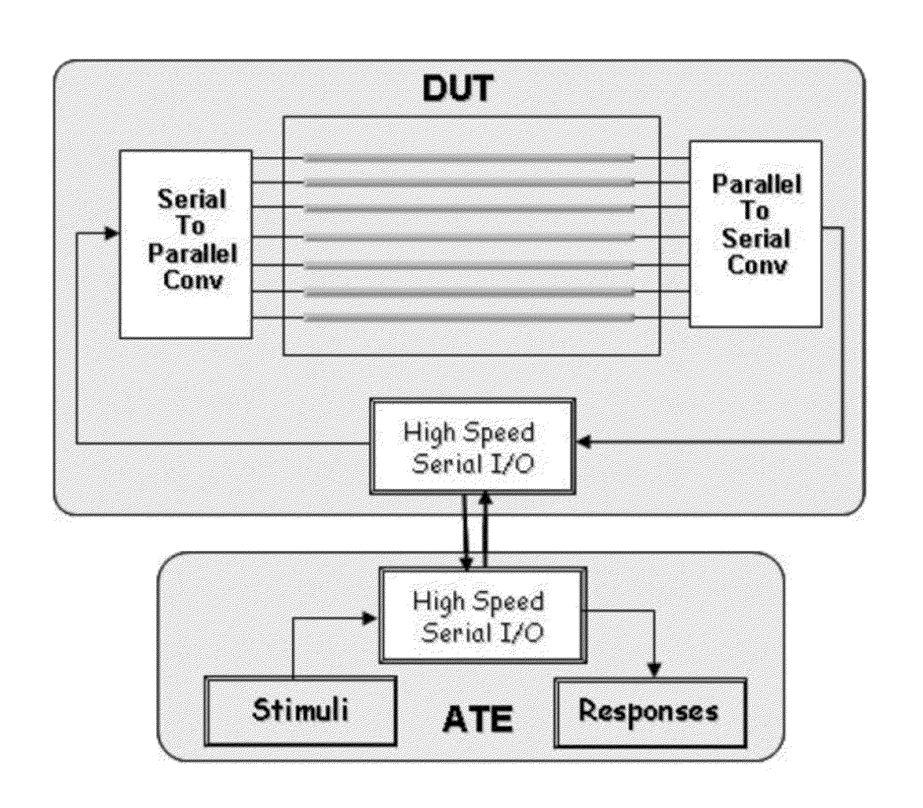
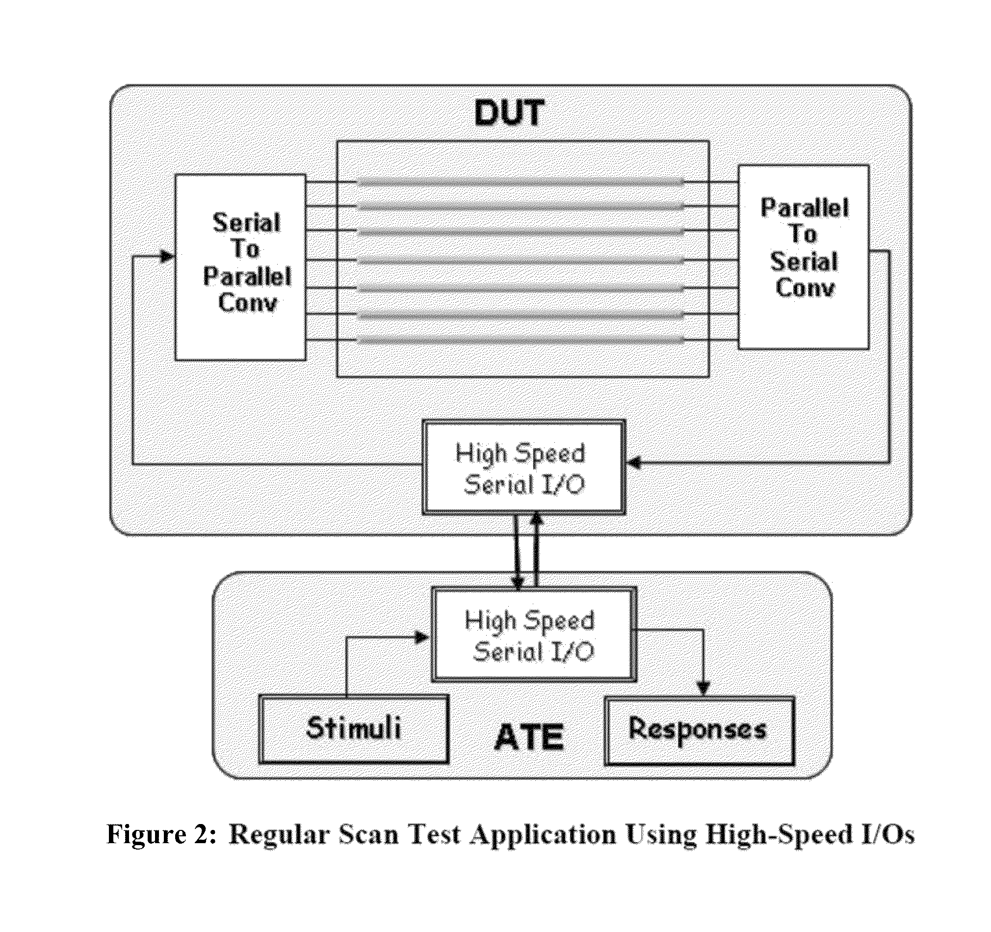
Scan test application through high-speed serial input/outputs
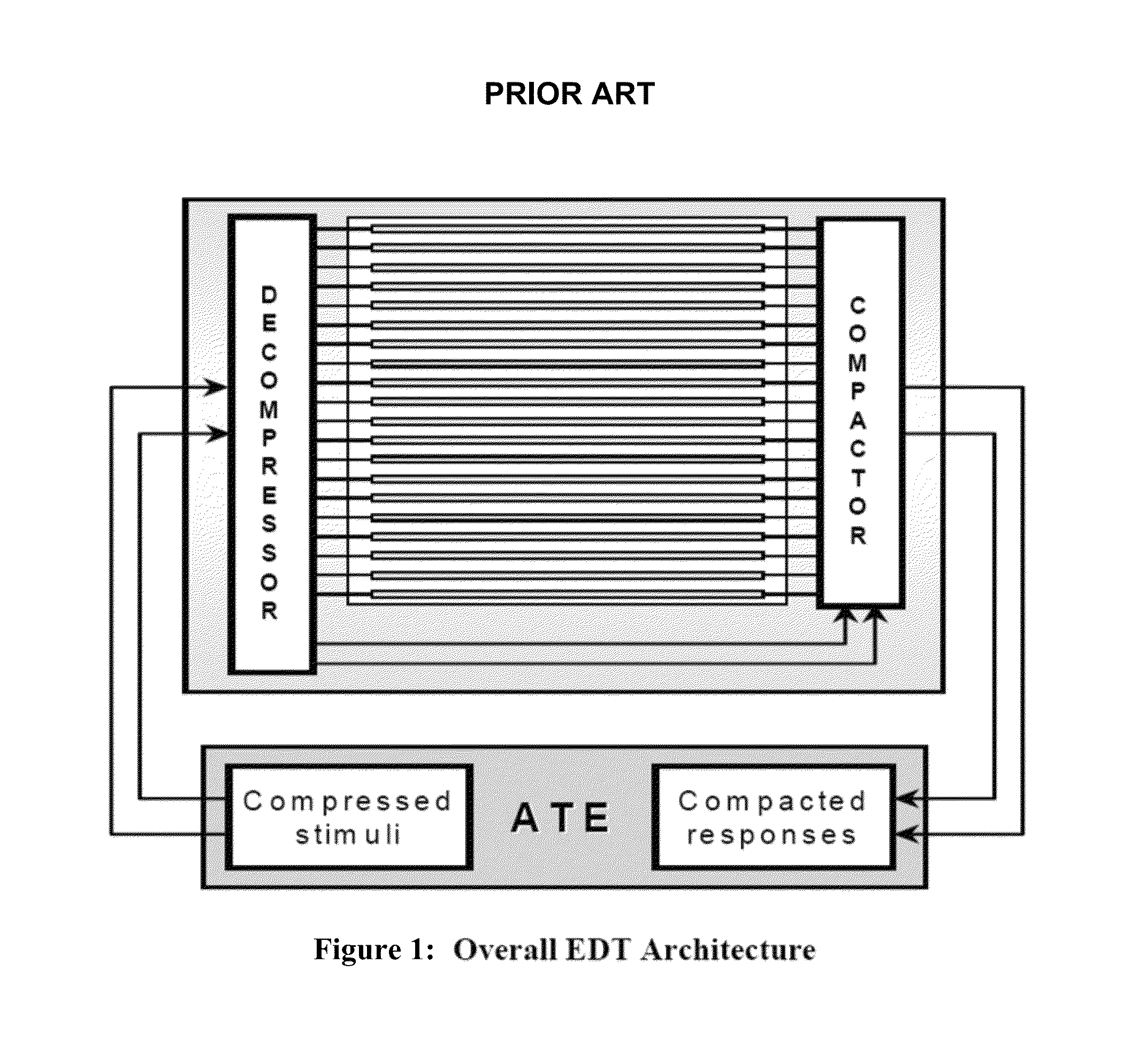
a high-speed, serial input technology, applied in the direction of electronic circuit testing, measurement devices, instruments, etc., can solve the problems of increasing the overall test application time, reducing the test data volume, and no longer providing a reliable, cost-effective means for keeping signals synchronized.
- Summary
- Abstract
- Description
- Claims
- Application Information
AI Technical Summary
Benefits of technology
Problems solved by technology
Method used
Image

Examples
Embodiment Construction
General Considerations
[0035]Disclosed below are representative embodiments of methods, apparatus, and systems for performing scan testing using high-speed serial link interfaces, such as scan testing between a device-under-test and automatic test equipment, which should not be construed as limiting in any way. Instead, the present disclosure is directed toward all novel and nonobvious features and aspects of the various disclosed methods, apparatus, and systems, alone and in various combinations and subcombinations with one another. Also, the disclosed technology is not limited to any specific aspect or feature, or combination thereof, nor do the disclosed methods, apparatus, and systems require that any one or more specific advantages be present or problems be solved. Any of the methods, apparatus, and systems described herein can be used in conjunction with a wide variety of scan-based or partially-scan-based circuits can be tested using automatic test equipment.
[0036]Although the...
PUM
 Abstract
Description
Claims
Application Information