

Film-forming method for forming passivation film and manufacturing method for solar cell element
a technology of passivation film and manufacturing method, which is applied in the direction of final product manufacturing, sustainable manufacturing/processing, pv power plants, etc., can solve the problems of loss of output characteristics of solar cell elements, and achieve excellent effect of improving output characteristics, satisfactory film quality of the resulting passivation film, and satisfactory film quality of the passivation film
- Summary
- Abstract
- Description
- Claims
- Application Information
AI Technical Summary
Benefits of technology
Problems solved by technology
Method used
Image


Examples
example 1
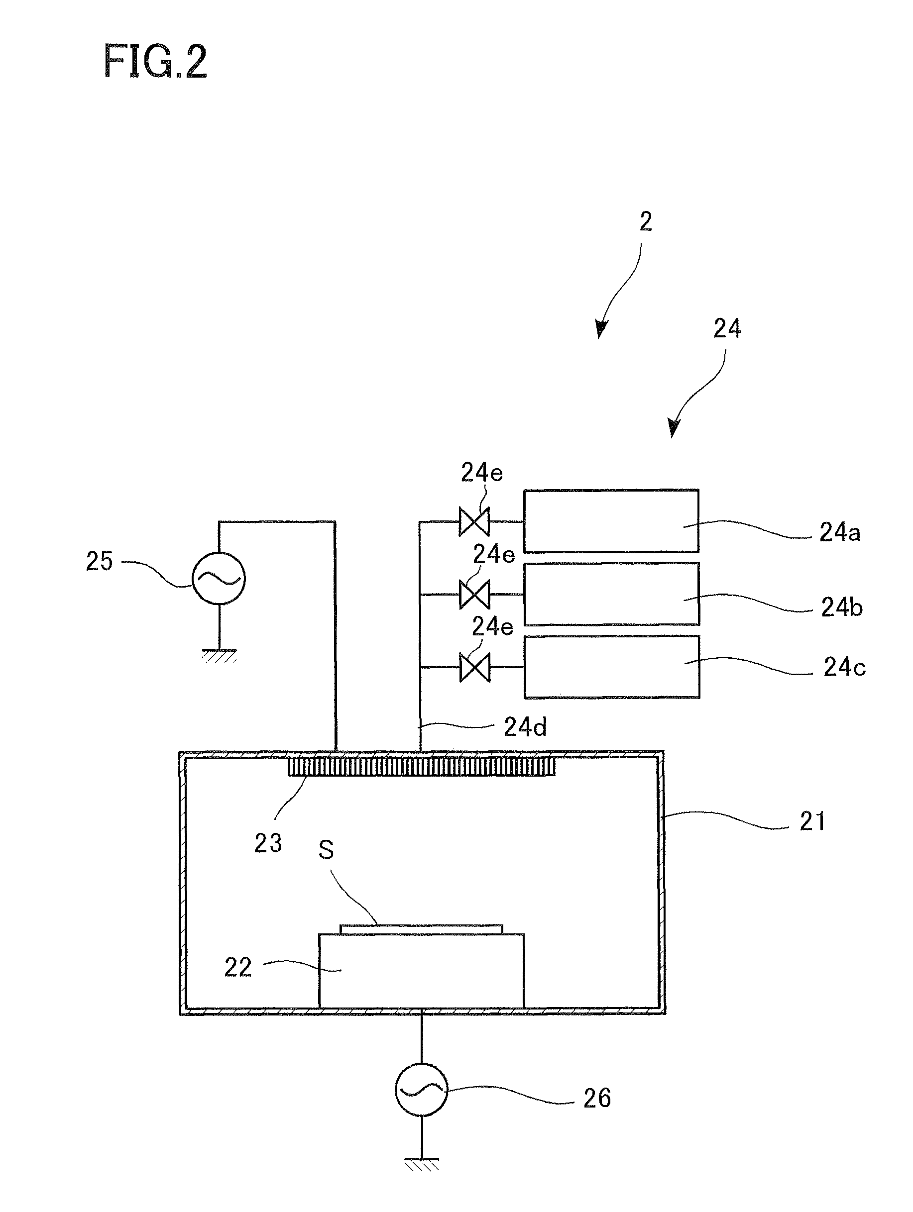
[0039]In the present example, a passivation film was formed using the film-forming device 2 shown in FIG. 2, whereafter a solar cell element was prepared.
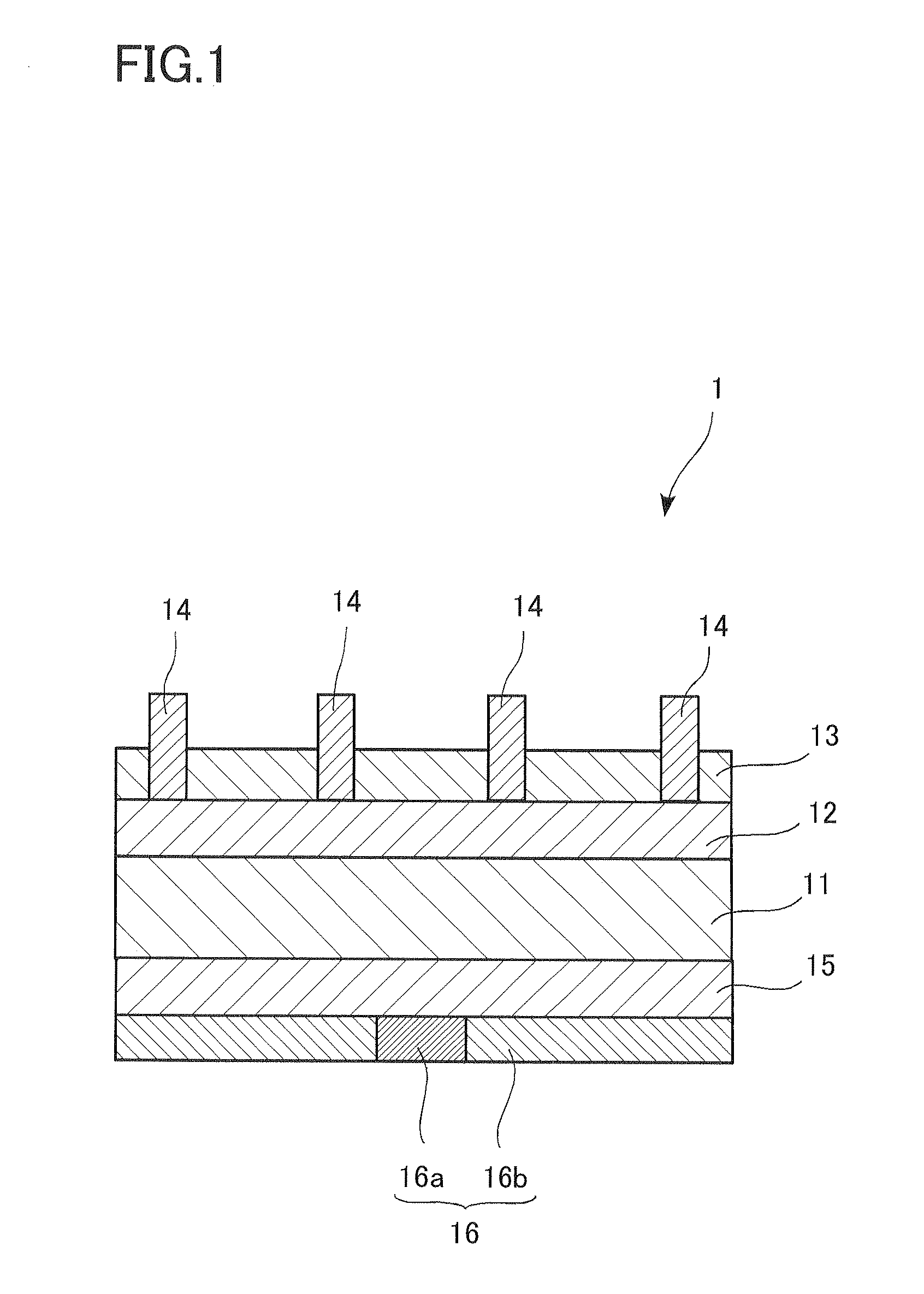
[0040]First, an n-type diffusion layer 12 was formed on a surface of a 220 μm thick p-type semiconductor substrate 11 (156 mm×156 mm) of monocrystal silicon having irregularities provided on the surface by texture etching. A plurality of the so treated substrates 11 were arranged side by side on a tray to provide a film-forming object S.
[0041]Then, the film-forming object S was carried into the film-forming device 2 shown in FIG. 2, and a passivation film comprising a silicon nitride film was formed under the following conditions: Substrate temperature: 350° C., SiH4 flow rate: 1500 sccm, NH3 flow rate: 5000 sccm, N2 flow rate: 6000 sccm, frequency of the high frequency power source 25: 13.56 MHz, inputting power of the high frequency power source 25: 1500 W, pressure within the vacuum chamber: 100 Pa, E / S: 14 mm, frequency of the ...
example 2
[0044]In the present example, a solar cell element 1 was produced under exactly the same conditions as those in Example 1, except that the inputting power of the low frequency power source 26 was set at 1000 W.
example 3
[0045]In the present example, a solar cell element 1 was produced under exactly the same conditions as those in Example 1, except that a passivation film was formed using the film-forming device 3 shown in FIG. 3.
PUM
| Property | Measurement | Unit |
|---|---|---|
| frequency | aaaaa | aaaaa |
| frequency | aaaaa | aaaaa |
| pressure | aaaaa | aaaaa |
Abstract
Description
Claims
Application Information