Method to grow group III-nitrides on copper using passivation layers

Active Publication Date: 2014-06-03
NAT TECH & ENG SOLUTIONS OF SANDIA LLC
View PDF0 Cites 1 Cited by
  • Summary
  • Abstract
  • Description
  • Claims
  • Application Information

AI Technical Summary

Benefits of technology

[0006]For example and as described in detail below, copper can be a suitable substrate material for c-plane GaN epitaxy using metal-organic chemical vapor deposition. By using a low temperature AlN passivation layer, Ga and Cu alloying can be prevented so that GaN layer can be grown on Cu at a temperature of 1000° C. As an example, an epitaxial relation of GaN (0001)//Cu(110) was observed using cros

Problems solved by technology

Due to the lack in availability and high prices of bulk GaN substrates, GaN is typically grown heteroepitaxially on foreign substrates, such as sapphire, SiC, and Si.
When these devices are operated in high power conditions, their performance is often limited by the

Method used


Image

  • Method to grow group III-nitrides on copper using passivation layers
  • Method to grow group III-nitrides on copper using passivation layers
  • Method to grow group III-nitrides on copper using passivation layers

Examples


Example

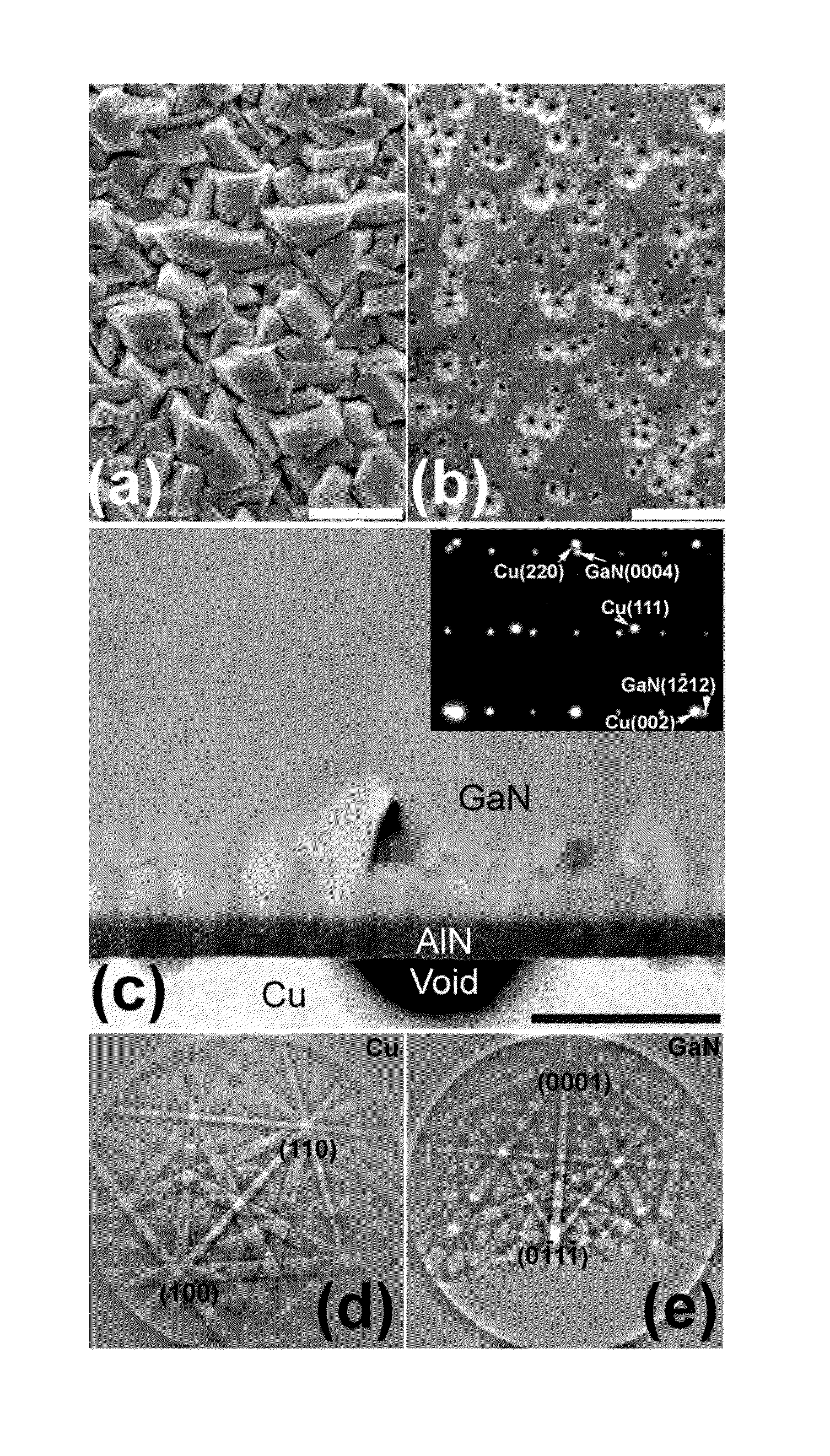
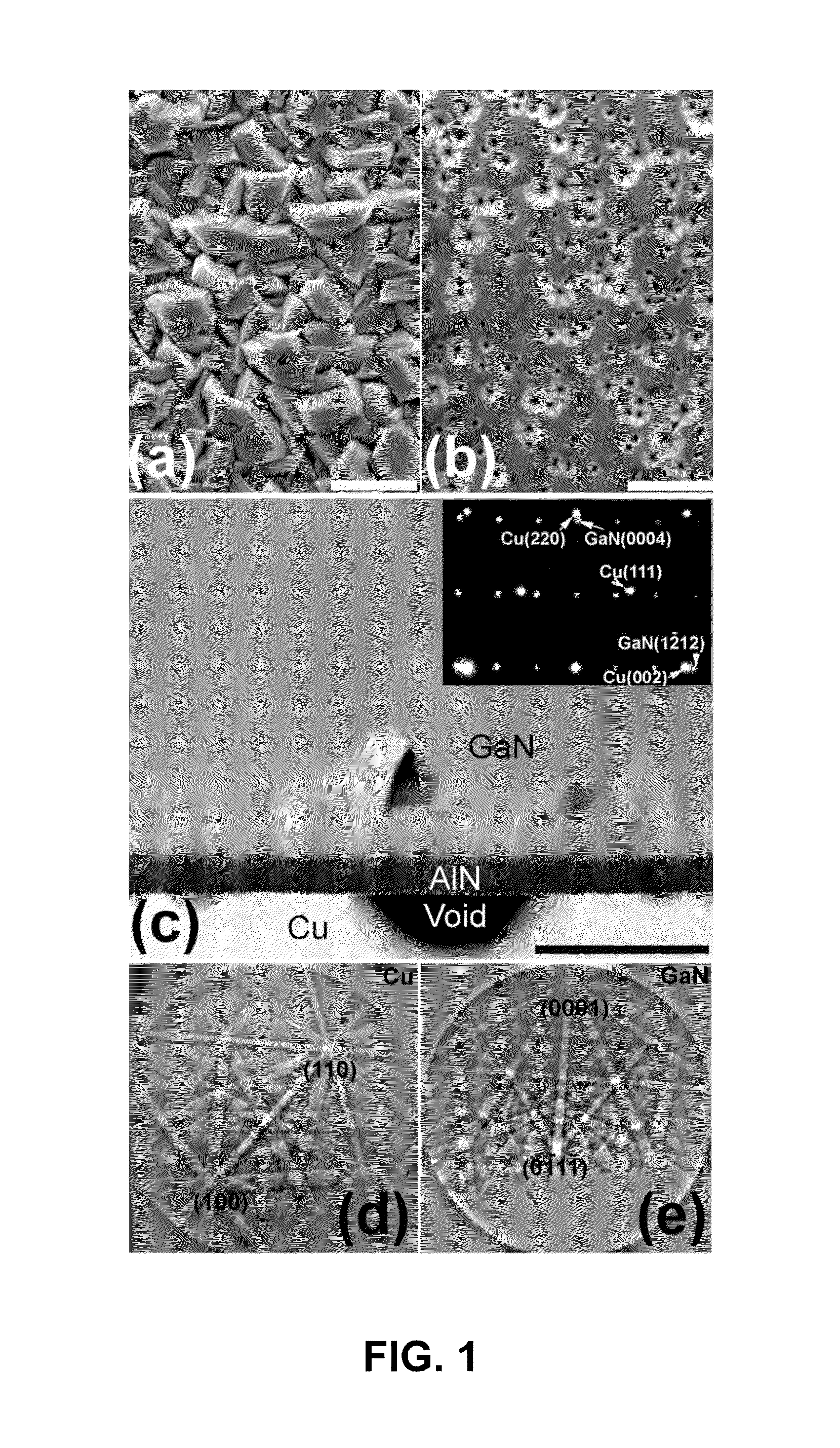
[0011]The present invention is directed to a method for growing Group III-nitride semiconductor materials on copper substrates using MOCVD because of the superior thermal and electrical conductivity of copper. The method comprises providing a copper substrate; growing a passivation layer on the copper substrate; and growing a Group III-nitride epilayer on the passivation layer. The copper substrate can comprise crystalline copper, such as single crystal Cu (110), Cu(100), or Cu(111), or oriented polycrystalline copper. For example, the passivation layer can comprise AlN, SiN, or TiN or compounds thereof with the main function of preventing alloying between the Group III element (e.g., gallium, indium, or aluminum) and copper. For example, the passivation layer can be grown by physical vapor deposition, chemical vapor deposition, metal-organic chemical vapor deposition, sputtering, reactive sputtering, or pulsed laser deposition. Typically, the passivation layer can have a thickness ...


PUM


Abstract

Group III-nitride epilayers can be grown directly on copper substrates using intermediate passivation layers. For example, single crystalline c-plane GaN can be grown on Cu (110) substrates with MOCVD. The growth relies on a low temperature AlN passivation layer to isolate any alloying reaction between Ga and Cu.

Description

STATEMENT OF GOVERNMENT INTEREST[0001]This invention was made with Government support under contract no. DE-AC04-94AL85000 awarded by the U.S. Department of Energy to Sandia Corporation. The Government has certain rights in the invention.FIELD OF THE INVENTION[0002]The present invention relates to Group III-nitride semiconductor growth and, in particular, to a method to grow Group III-nitrides on copper using passivation layers.BACKGROUND OF THE INVENTION[0003]Gallium nitride and its aluminum and indium compound semiconductor alloys have been a focus of intense research effort because of their importance in light-emitting, lasing, high-frequency, high mobility, and high-power devices. Due to the lack in availability and high prices of bulk GaN substrates, GaN is typically grown heteroepitaxially on foreign substrates, such as sapphire, SiC, and Si. When these devices are operated in high power conditions, their performance is often limited by the poor electrical and thermal conducti...

Claims


Application Information

Patent Timeline
IPC IPC(8): H01L21/36
CPCH01L21/02488H01L21/02458H01L21/0254H01L21/02433H01L21/02425H01L21/0262H01L21/02491C30B25/18C30B25/183C30B29/403C30B29/406
Inventor LI, QIMINGWANG, GEORGE T.FIGIEL, JEFFREY T.
Owner NAT TECH & ENG SOLUTIONS OF SANDIA LLC
Why Eureka
Try Eureka