Laminated electronic component and manufacturing method thereof

a technology of laminated electronic components and manufacturing methods, which is applied in the direction of transformers/inductances, magnets, magnetic cores, etc., can solve the problems of increasing the cost of the screen, increasing the cost of the product, and unfailingly preventing cracking and shorting by the method described in the patent literature 2 above, so as to reduce the proportion of the internal conductor at the connection part to that at the non-connection part, the effect of preventing the cracking of th

Active Publication Date: 2014-06-10
TAIYO YUDEN KK
View PDF9 Cites 11 Cited by
  • Summary
  • Abstract
  • Description
  • Claims
  • Application Information

AI Technical Summary

Benefits of technology

[0017]According to the present invention, in a laminated electronic component constituted by multiple laminated insulator layers, each with wires comprising conductors formed on the surface, adjacent wires sandwiching each insulator layers are connected by a connection conductor formed in a manner filling inside and projecting on top of a via hole penetrating through the insulator layer. Additionally, the connection conductor is shaped in such a way that its center is recessed to become lower than the outer periphery of the via hole. As a result, the proportion of the internal conductor at the connection part to that at the non-connection part is lowered, and consequent cracking can be prevented. In addition, less material is required because the amount of internal conductor at the connection part is reduced. Furthermore, shorting defects can be prevented by thickly forming the insulator layer between the connection conductor and adjacent wires.

Problems solved by technology

However, the technology described in Patent Literature 2 specified above requires changing the screen manufacturing method to partially change the screen opening ratio, and has problems such as making the screen more expensive and adding to the cost of the product.
40 μm, unfailingly preventing cracking and shorting by the method described in Patent Literature 2 above has been difficult.

Method used


Image

  • Laminated electronic component and manufacturing method thereof
  • Laminated electronic component and manufacturing method thereof
  • Laminated electronic component and manufacturing method thereof

Examples


example 1

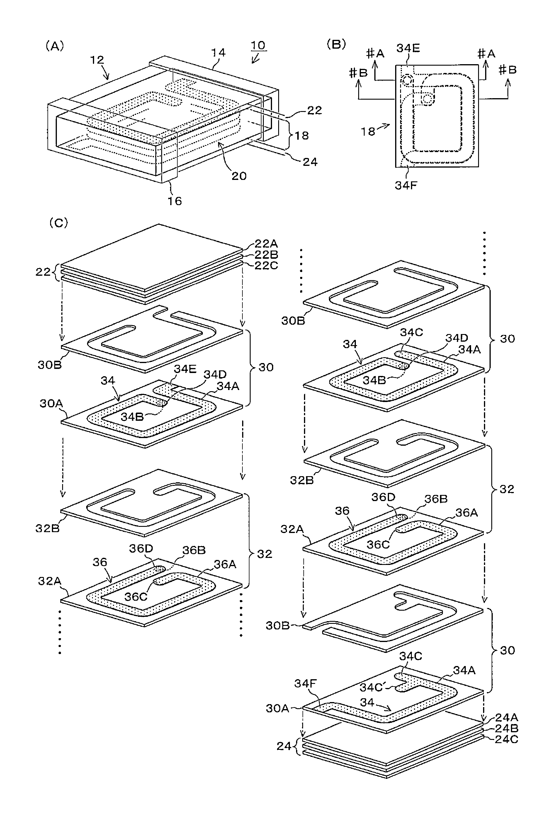
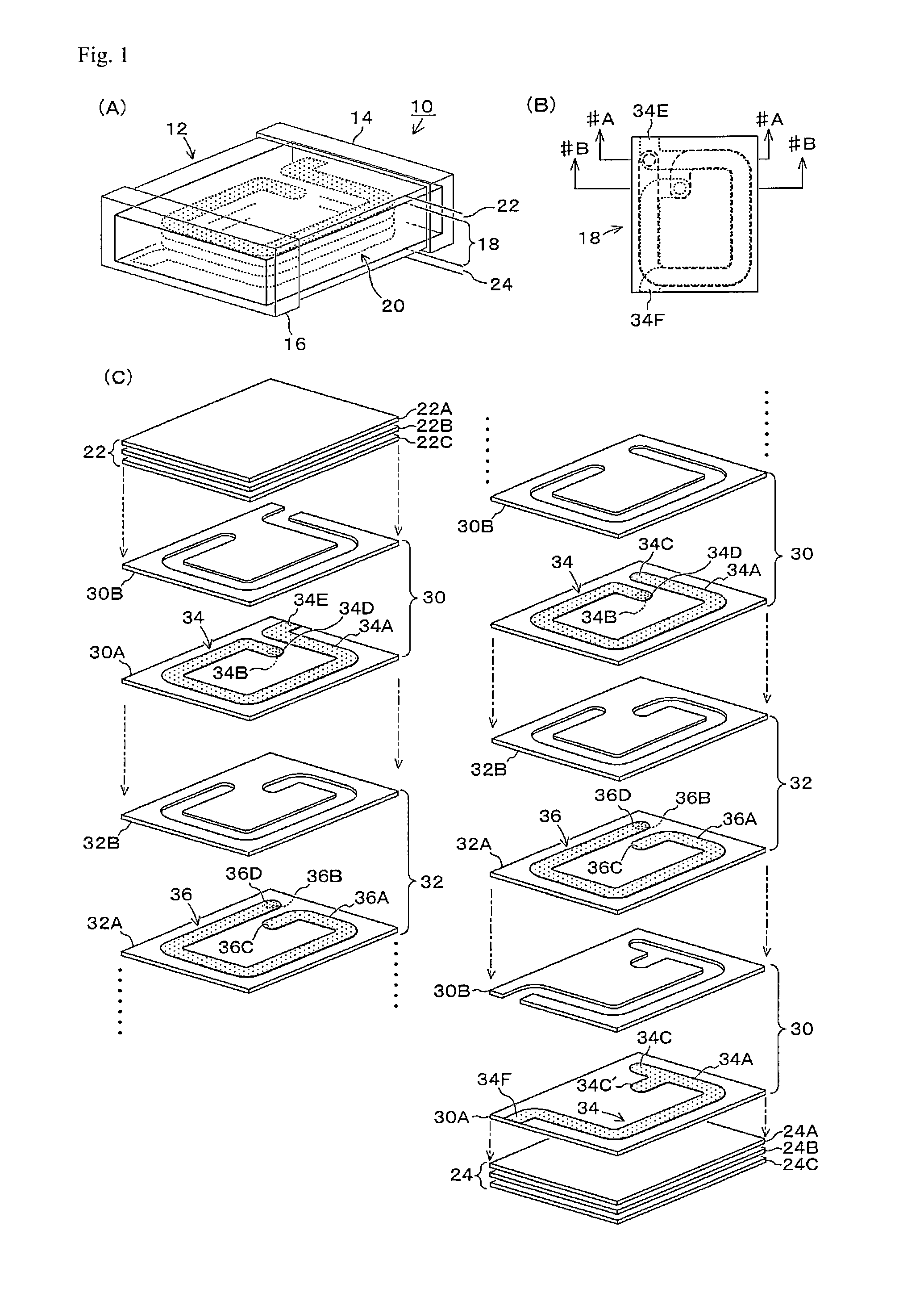
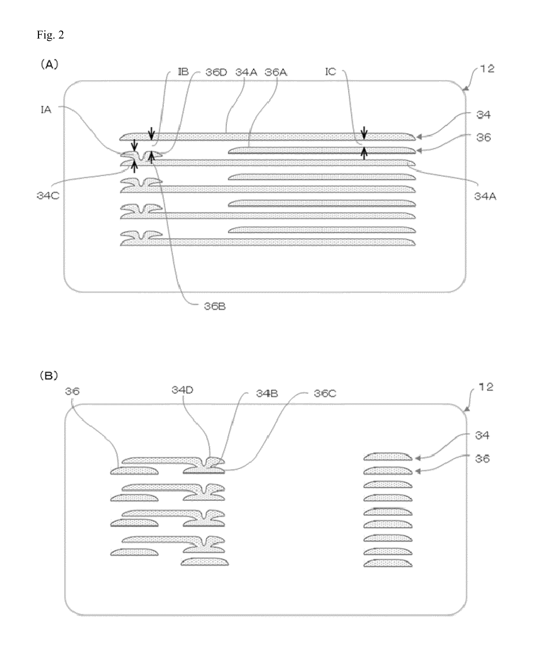
[0062]First, the structure of the laminated chip inductor in this example is explained by referring to FIGS. 1 and 2. The present invention can be applied to all laminated electronic components having a laminated wire structure, but this example is explained by citing, as an example, a laminated chip inductor having a spiral coil conductor formed in an insulator. FIG. 1(A) is an external perspective view of the laminated chip inductor in this example, FIG. 1(B) is a plan view of its laminate, and FIG. 1(C) is a perspective view showing the condition of the laminate before lamination. FIG. 2(A) is a section view of FIG. 1(B) above, cut along line #A-#A and viewed in the direction of the arrow, while FIG. 2(B) is a section view of FIG. 1(B) above, cut along line #B-#B and viewed in the direction of the arrow. As shown in FIG. 1(A), the laminated chip inductor 10 in this example has a structure whereby external electrodes 14, 16 are formed on both end faces of a laminate 12 that sandwi...


PUM

PropertyMeasurementUnit
thicknessaaaaaaaaaa
widthaaaaaaaaaa
widthaaaaaaaaaa

Abstract

A laminated electronic component with adjacent wires (such as coil conductors) in insulator layers inter-connected through via holes, wherein its laminate is structured in such a way that a coil-embedded layer constituted by first insulator layers and second insulator layers laminated alternately is sandwiched between a top magnetic layer and bottom magnetic layer, with external electrodes formed on both end faces. First coil conductors are formed on the first insulator layers and second coil conductors are formed on the second insulator layers, with these coil conductors connected through via holes. Formed at the end of each second coil conductor is a connection conductor of a size sufficiently large to block off the top of the via hole provided in the insulator sheet. By discharging the air in the via hole by means of pressure-bonding the laminate, the connection conductor will have a part filling inside the via hole and another part projecting on top of the via hole, with the center of the via hole recessed, to prevent shorting and cracking.

Description

BACKGROUND[0001]1. Field of the Invention[0002]The present invention relates to a laminated electronic component and manufacturing method thereof, and more specifically to improvement of component reliability.[0003]2. Description of the Related Art[0004]Laminated electronic components, each formed by laminating multiple insulator layers with a pattern constituting a part of a coil conductor formed on the surface, and then connecting the patterns through via holes, thereby forming a spiral coil conductor, are utilized in various applications. Such laminated electronic components are facing the demand for component size reduction as the devices in which they are utilized become smaller, more power-efficient and higher-performance, and, in particular, laminated electronic components used as inductors in power circuits are asked to offer lower resistivity. The easiest way to reduce the resistance of a laminated electronic component is to increase the thickness of its internal conductor,...

Claims


Application Information

Patent Timeline
Patent Type & Authority Patents(United States)
IPC IPC(8): H01F5/00H01F27/24H01F27/02
CPCH01F2017/0066H01F27/2804H01F17/0013H01F41/041H01F41/046Y10T29/4902
Inventor TAKAHASHI, OSAMU
Owner TAIYO YUDEN KK
Why Eureka
Try Eureka