Method of manufacturing semiconductor device including ashing of photoresist with deuterium or tritium gas

a technology of photoresist and semiconductor, applied in the field of semiconductor processing technology, can solve the problems of reducing unable to eliminate negative effects, and unable to meet current process requirements, so as to reduce or eliminate the generation of si recesses and improve the performance of the semiconductor device.

Active Publication Date: 2014-06-17
SEMICON MFG INT (SHANGHAI) CORP
View PDF6 Cites 0 Cited by
  • Summary
  • Abstract
  • Description
  • Claims
  • Application Information

AI Technical Summary

Benefits of technology

[0011]Embodiments of the present invention provide a method of manufacturing a semiconductor device capable of reducing the loss of Si and silicon nitride during an ashing process.
[0020]In the method of manufacturing a semiconductor device according to one embodiment of this disclosure, a photo resist is ashed using a gas mixture comprising a D2 or T2 gas. The method reduces or eliminates the generation of Si recess and the loss of silicon nitride thin film, thereby improving the performance of the semiconductor device.

Problems solved by technology

The main problems include Si recess and a film property change, which may lead to issues of LDD litho patterning scrumming, and have difficulty to meet current process requirements.
Although the process reduces the loss of Si, it cannot eliminate negative effects such as the loss of the silicon nitride offset spacer and the like.
Then, the loss of silicon nitride spacer will become more serious.
In the photo resist stripping process after an LDD implantation, the O2 rich ashing does not generate residues, however, the result of Si recess is far from satisfactory.
But the reaction between Si- and H-results in a severe loss of silicon nitride offset spacer; in some cases, the silicon nitride offset spacer is even removed, as shown in the circle on diagram “b” of FIG. 1.

Method used


Image

  • Method of manufacturing semiconductor device including ashing of photoresist with deuterium or tritium gas
  • Method of manufacturing semiconductor device including ashing of photoresist with deuterium or tritium gas
  • Method of manufacturing semiconductor device including ashing of photoresist with deuterium or tritium gas

Examples


first embodiment

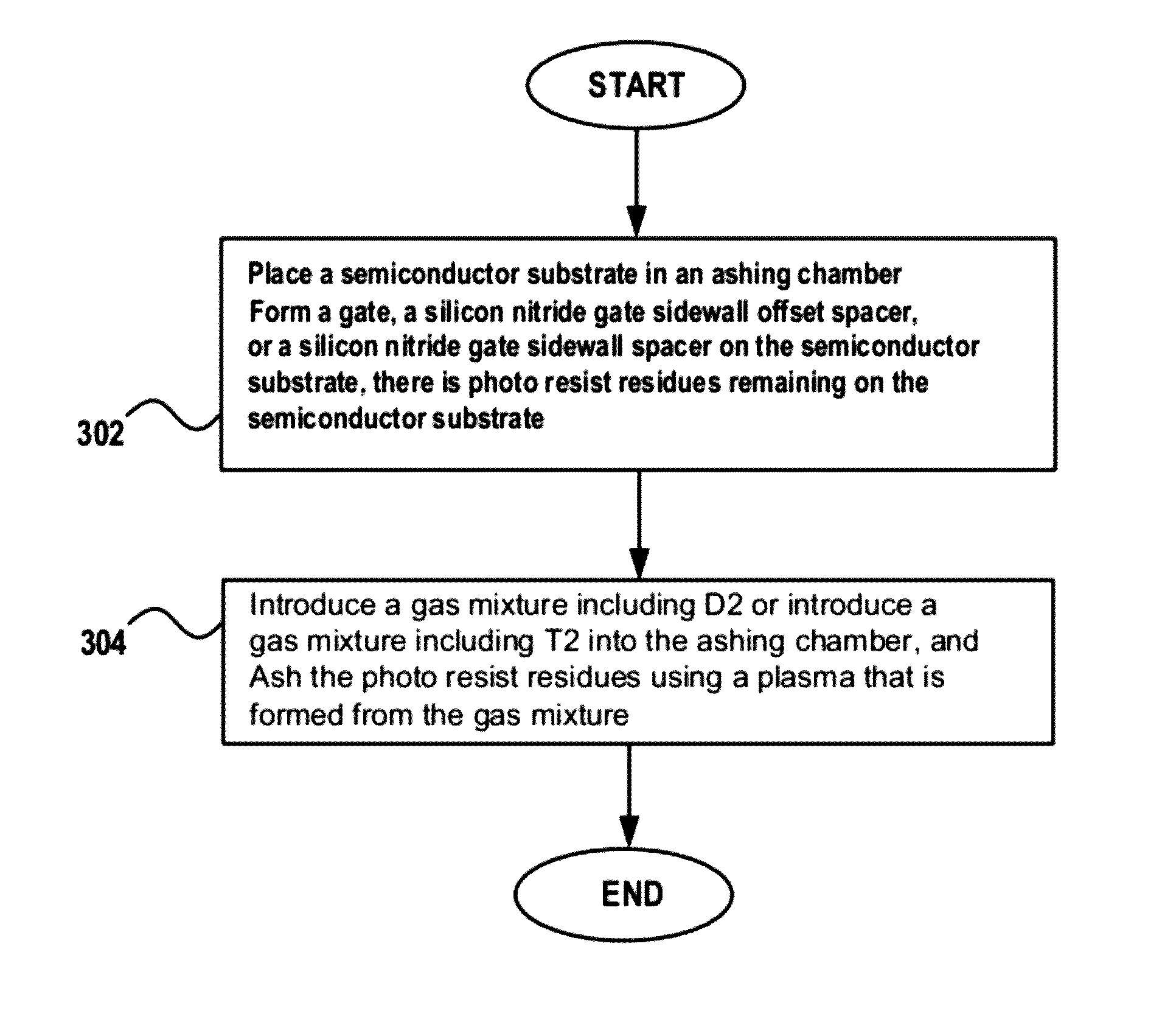
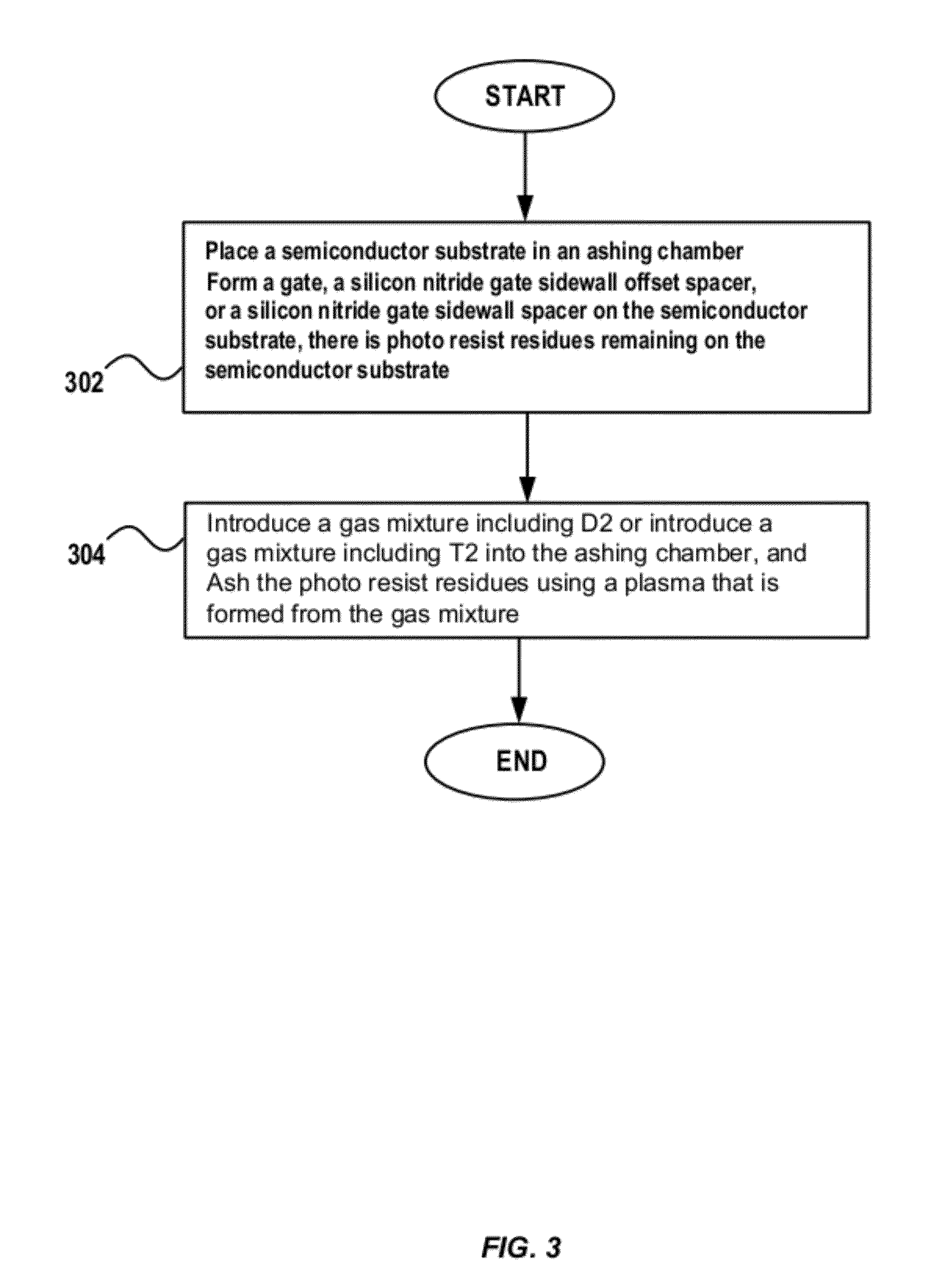
[0033]FIG. 3 shows a flowchart diagram of a method of manufacturing a semiconductor device according to the present invention. As shown in FIG. 3, a semiconductor substrate is placed in an ashing chamber (step 302). A gate, a silicon nitride gate sidewall offset spacer or a silicon nitride gate sidewall spacer can be formed on the semiconductor substrate. There are photo resist residues remaining on the semiconductor substrate. The photo resist residues can be the residuals after an etching or an implantation process.

[0034]At step 304, a gas mixture including D2 or a gas mixture including T2 can be introduced into the ashing chamber, and the photo resist residues can be ashed using a plasma that is formed from the gas mixture. In an embodiment, the gas mixture including D2 can include D2 and N2. In another embodiment, the gas mixture including D2 can include D2 and an inert gas (e.g., He, Ar). Similarly, the gas mixture including T2 can include T2 and N2, or the as mixture including...

second embodiment

[0038]FIG. 4 shows a flowchart diagram illustrating a method 400 of manufacturing a semiconductor device according to the present invention.

[0039]As shown in FIG. 4, a polysilicon gate can be formed on a semiconductor substrate (step 402). At step 404, a silicon nitride layer can be deposited on the semiconductor substrate and on the polysilicon gate.

[0040]At step 406, the silicon nitride layer can be etched to form a silicon nitride gate sidewall offset spacer on each side of the polysilicon gate.

[0041]At step 408, a photo resist layer can be coated on the semiconductor substrate including the polysilicon gate and the silicon nitride gate sidewall offset spacer.

[0042]At step 410, the photo resist layer is patterned to form a lightly doped drain region.

[0043]At step 412, an LDD implantation can be performed using the patterned photo resist layer. The LDD implantation can be a high dose implantation, or medium, low dose implantation.

[0044]At step 413, ashing can be performed using th...

third embodiment

[0047]FIG. 5 shows a flowchart diagram illustrating a method 500 of manufacturing a semiconductor device according to the present invention.

[0048]As shown in FIG. 5, a gate can be formed on a semiconductor substrate, the gate has sidewalls that are substantially vertical (step 502).

[0049]At step 504, an LDD implantation can be performed in the semiconductor substrate to form LDD regions at both sides of the gate using the gate as a mask.

[0050]At step 506, a silicon nitride layer can be deposited on the semiconductor substrate including the gate.

[0051]At step 508, the silicon nitride layer can be etched to form a silicon nitride gate sidewall spacer on each sidewall of the gate.

[0052]At step 510, a photo resist layer can be coated on the semiconductor substrate including the gate and the silicon nitride gate sidewall spacers.

[0053]At step 512, the photo resist layer can be patterned.

[0054]At step 514, a source and a drain implantation can be performed in the semiconductor substrate u...


PUM

PropertyMeasurementUnit
pressureaaaaaaaaaa
temperatureaaaaaaaaaa
sizesaaaaaaaaaa

Abstract

A method of manufacturing a semiconductor device comprises placing a semiconductor substrate in an ashing chamber, the semiconductor substrate having a gate, a silicon nitride gate sidewall offset spacer or a silicon nitride gate sidewall pacer formed thereon, and a photo resist residue remaining on the semiconductor substrate, introducing a gas mixture including D2 or T2 into the ashing chamber, and ashing the photo resist residue using a plasma that is formed from the gas mixture. The gas mixture can include a deuterium gas or a tritium gas having a volume ratio ranging between about 1% and about 20%. Embodiments can reduce Si recess and the loss of silicon nitride thin film during ashing.

Description

CROSS-REFERENCES TO RELATED APPLICATIONS[0001]This application claims priority to Chinese Patent Application No. 201110117450.5, filed on May 9, 2011 and entitled “METHOD OF MANUFACTURING SEMICONDUCTOR DEVICE”, which is incorporated herein by reference in its entirety.BACKGROUND OF THE INVENTION[0002]1. Field of the Invention[0003]The present invention relates to semiconductor processing technology, and more particularly, to a method of removing photo resist residues in the manufacturing of semiconductor devices.[0004]2. Description of the Related Art[0005]Photo resist, also called resist for short, is a macromolecular compound whose erosion resistance capacity will be changed after lighting. Photo resist is a photosensitive material. In some semiconductor manufacturing processes, a photo resist layer can be formed on a surface of a device (such as a semiconductor wafer), and a patterned photo resist can be formed after lithography. As such, the surface which is not covered by the p...

Claims


Application Information

Patent Timeline
Patent Type & Authority Patents(United States)
IPC IPC(8): H01L21/302H01L21/461H01L21/336
CPCH01L21/31138
Inventor MENG, XIAOYINGZHOU, JUNQINGZHANG, HAIYANG
Owner SEMICON MFG INT (SHANGHAI) CORP
Why Eureka
Try Eureka