

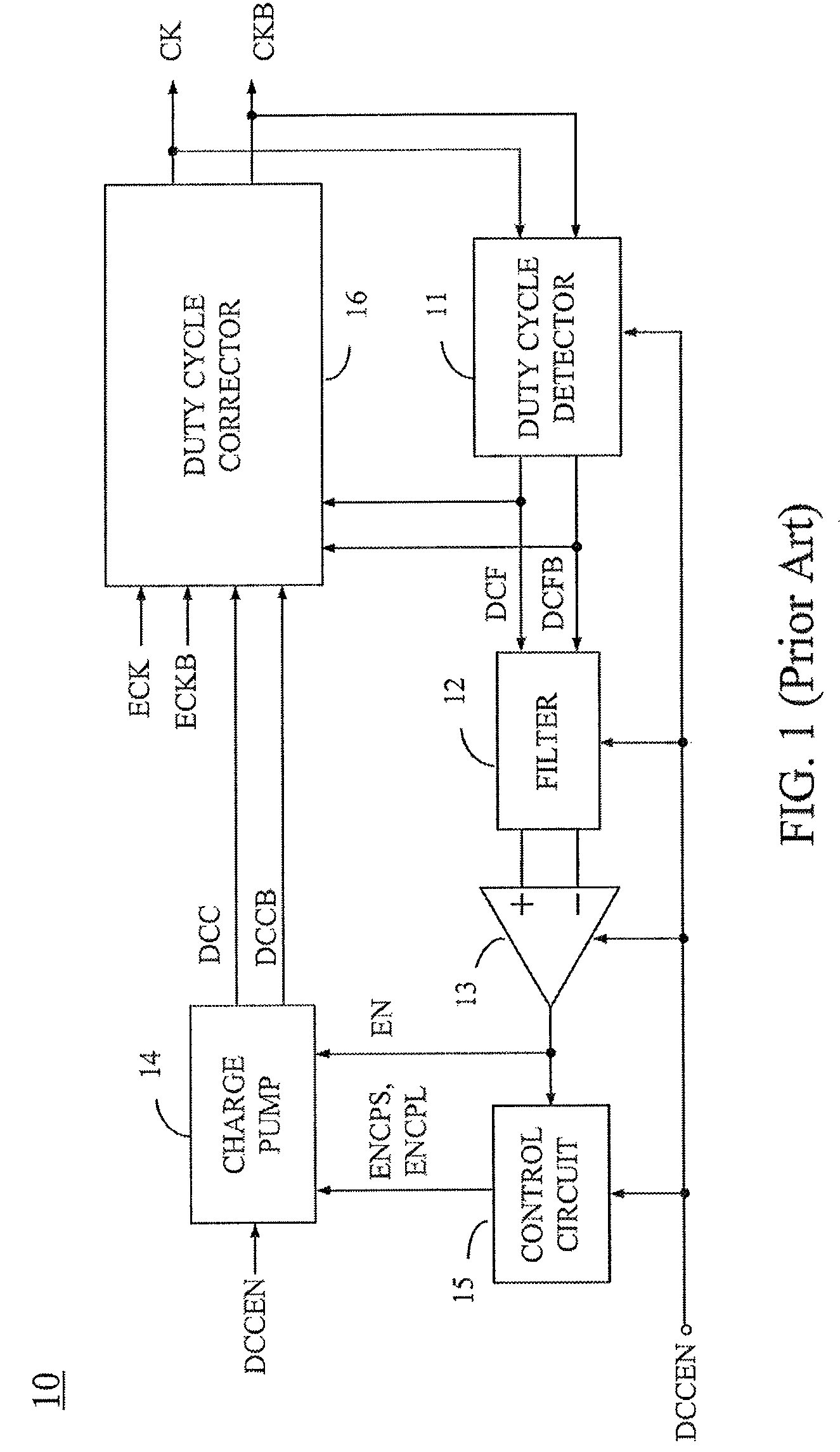
Duty cycle correction circuit
a duty cycle and circuit technology, applied in pulse manipulation, pulse duration/width modulation, pulse technique, etc., can solve the problems of large impact on the performance of ddr sdram, time delay, and design margin decreas
- Summary
- Abstract
- Description
- Claims
- Application Information
AI Technical Summary
Benefits of technology
Problems solved by technology
Method used
Image

Examples
first embodiment
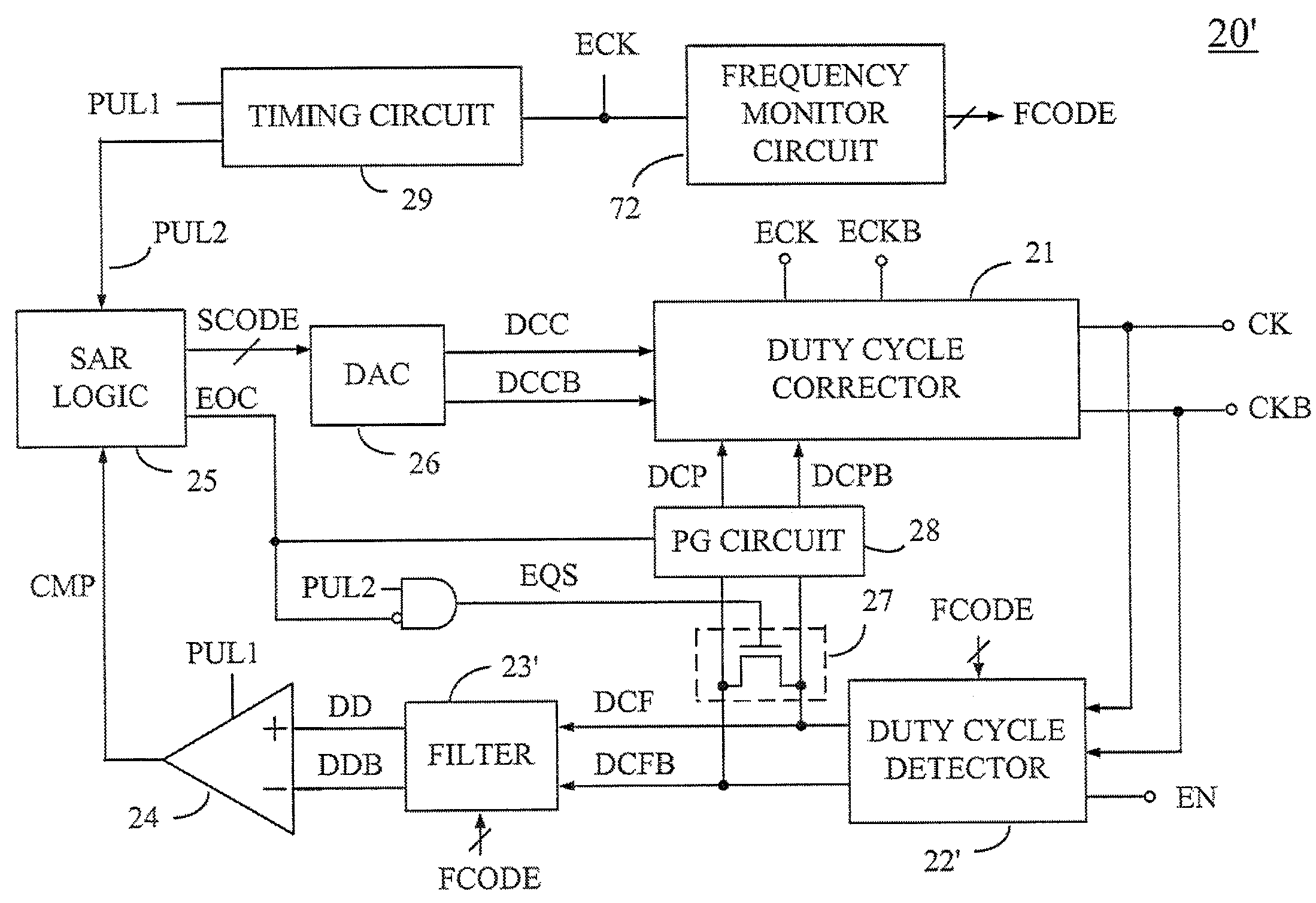
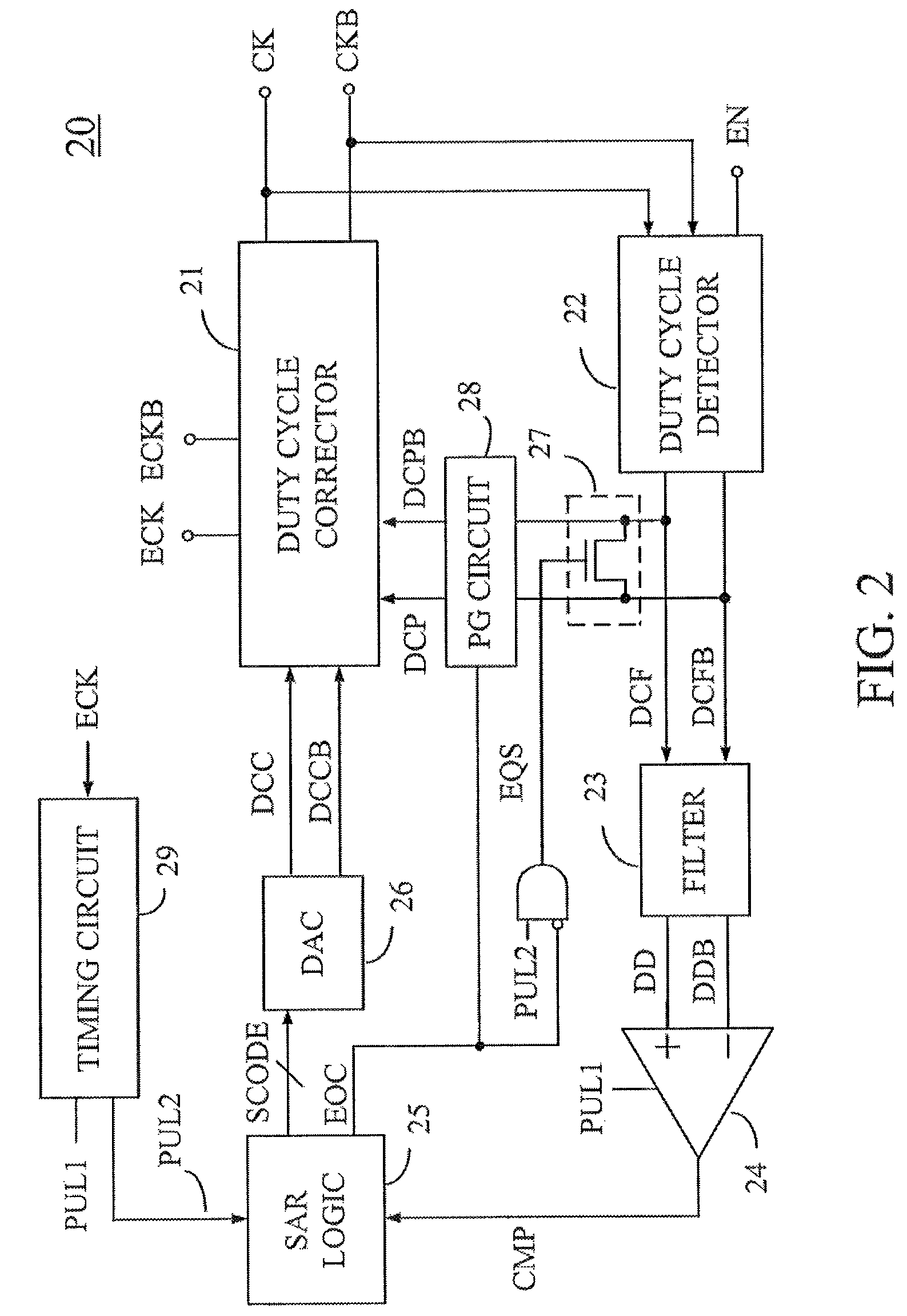
[0025]FIG. 2 shows a block diagram of a duty cycle correction circuit 20 according to the present invention. The duty cycle correction circuit 20 comprises a duty cycle corrector 21, a duty cycle detector 22, a filter 23, a comparator 24, a successive-approximation-register (SAR) logic 25, and a digital to analog converter (DAC) 26.
[0026]Referring to FIG. 2, the duty cycle corrector 21 generates a pair of internal clock signals CK and CKB in response to a pair of external clock signals ECK and ECKB, wherein the clock signal CKB is complementary to the clock signal CK and the clock signal ECKB is complementary to the clock signal ECK. The duty cycle detector 22 generates a pair of control signals DCF and DCFB based on the duty cycle of the pair of internal clock signals CK and CKB, wherein the control signal DCFB is complementary to the control signal DCF. The filter 23 filters the pair of control signals DCF and DCFB to obtain a pair of average signals DD and DDB, wherein the signal...
second embodiment
[0042]FIG. 8 shows a detailed block diagram of the frequency monitor circuit 72 according to at least the present invention. Referring to FIG. 8, the frequency monitor circuit 72 comprises a divider 722, a delay unit 724, and a comparison unit 726. The frequency divider 722 divides the frequency of the external clock signal ECK and outputs a divided clock signal DCK2. The delay unit 724 comprises a plurality of delay circuits, each of which delays the divided clock signal DCK2 by a corresponding time. The comparison unit 726 comprising a plurality of comparison circuits compares the divided clock signal DCK2 with the delayed signals from the delay unit 724 and generates the digital code FCODE representative of frequency distribution.
[0043]FIG. 9 is an operation waveform of the frequency monitor circuit 72 ofFIG. 7 in the case in which the clock speed of the external clock signal ECK is about 125 MHz. FIG. 10 is an operation waveform of the frequency monitor circuit 72 of FIG. 7 in t...
PUM
 Abstract
Description
Claims
Application Information