Method of forming a FinFET structure

a technology of non-planar transistors and fin structures, which is applied in the direction of basic electric elements, electrical apparatus, and semiconductor devices, can solve the problems of poor cd uniformity of the fin structure of the fin structure of the fin structure of the fin-fet, and the current planar fets no longer meet the requirements of the products, so as to improve the quality of the device

Active Publication Date: 2014-10-07
MARLIN SEMICON LTD
View PDF27 Cites 20 Cited by
  • Summary
  • Abstract
  • Description
  • Claims
  • Application Information

AI Technical Summary

Benefits of technology

[0010]By using the method set forth in the present invention, the CD of the fin structures can be uniform and the quality of the devices can be improved.

Problems solved by technology

However, with the increasing miniaturization of electronic products, current planar FETs no longer meet the requirements of the products.
However, some issues, such as poor CD uniformity of the fin structures of Fin-FETs, are still problems that should be overcome.

Method used


Image

  • Method of forming a FinFET structure
  • Method of forming a FinFET structure
  • Method of forming a FinFET structure

Examples


Embodiment Construction

[0014]To provide a better understanding of the present invention, preferred embodiments will be made in detail. The preferred embodiments of the present invention are illustrated in the accompanying drawings with numbered elements.

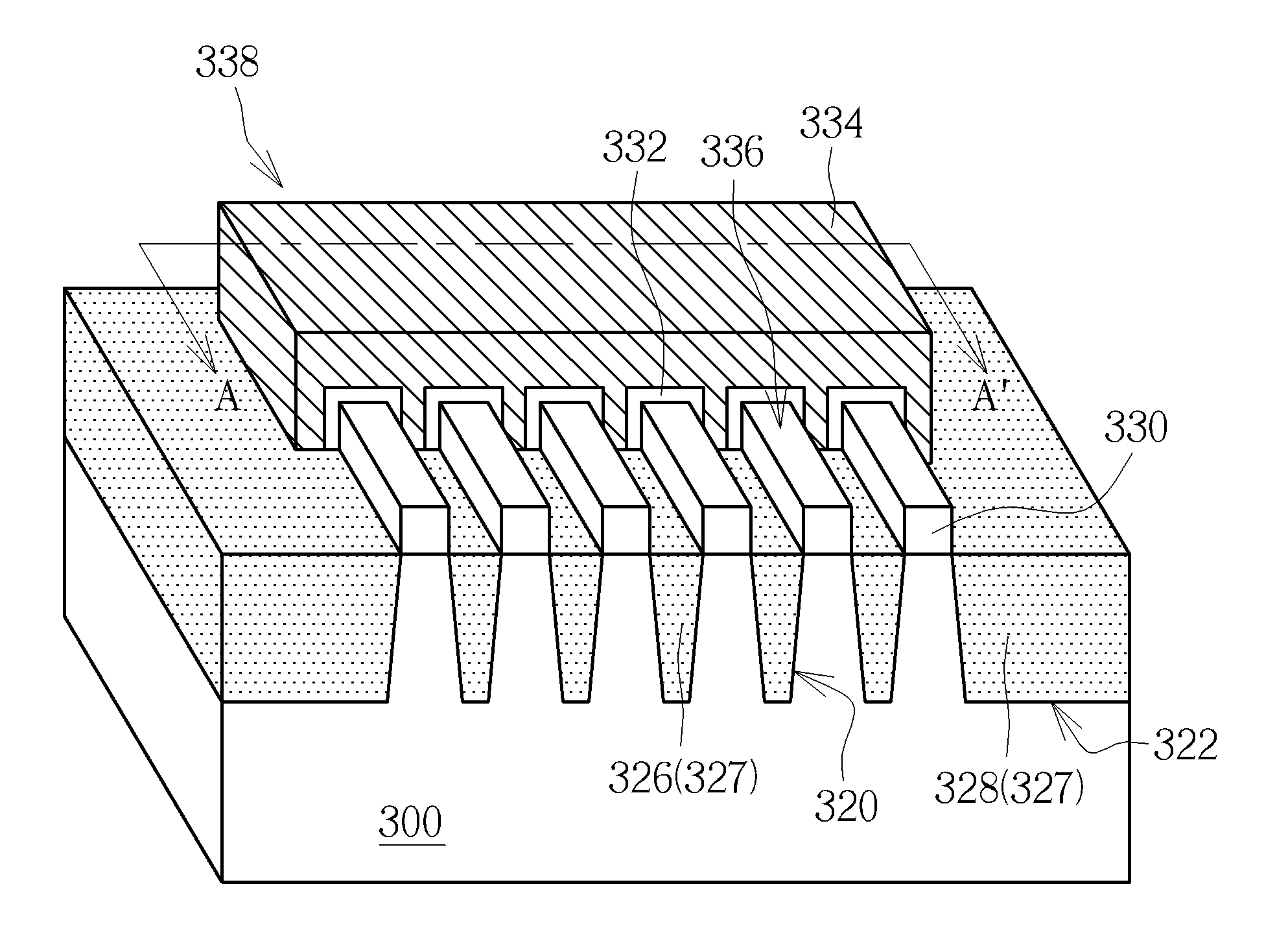
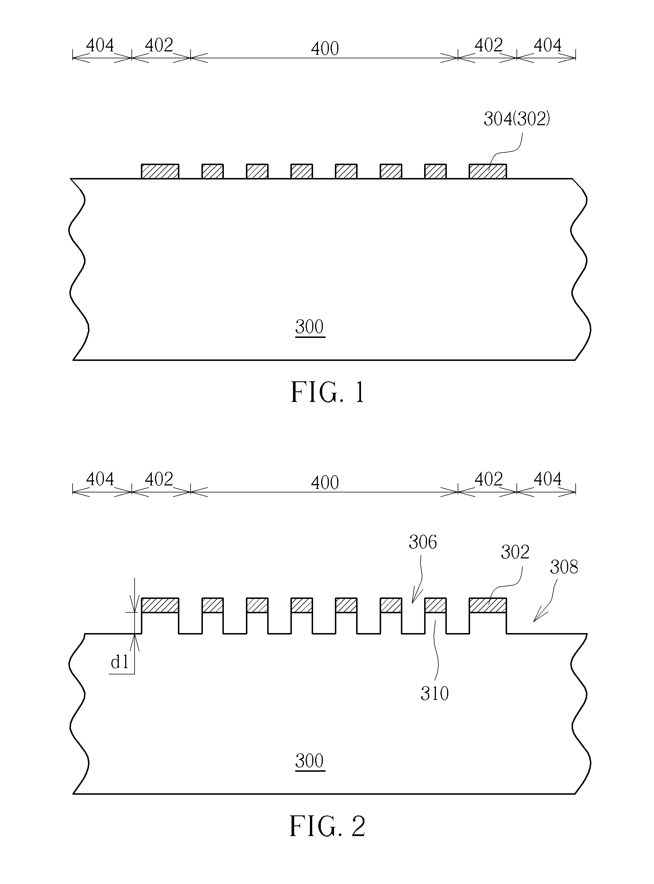
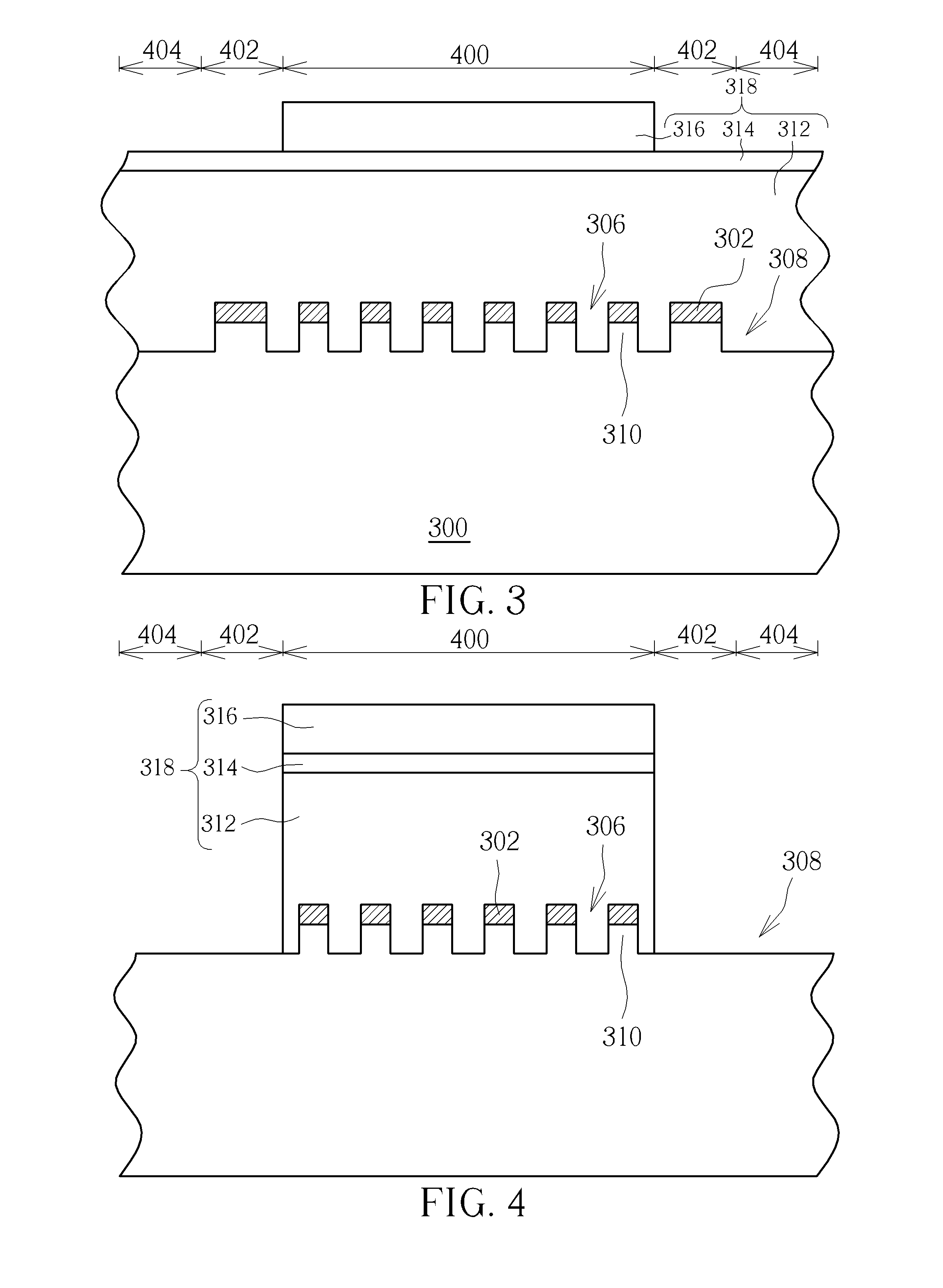
[0015]Please refer to FIG. 1 to FIG. 8, which are schematic diagrams of the fabrication method of a non-planar FET according to the first embodiment in the present invention. As shown in FIG. 1, a substrate 300 is provided. In one embodiment, the substrate 300 can be a silicon substrate, an epitaxial silicon substrate, a silicon germanium substrate or a silicon carbide substrate, but is not limited thereto. A first region 400, a second region 402 and a third region 404 are defined on the substrate 300. The second region 402 is disposed between the first region 400 and the third region 404 so that the second region 402 encompasses the first region 400, and the third region 404 encompasses both the first region 400 and the second region 402. A patterned mask...


PUM


Abstract

A method of forming a fin structure is provided. First, a substrate is provided, wherein a first region, a second region encompassing the first region, and a third region encompassing the second region are defined on the substrate. Then, a plurality of first trenches having a first depth are formed in the first region and the second region, wherein each two first trenches defines a first fin structure. The first fin structure in the second region is removed. Lastly, the first trenches are deepened to form a plurality of second trenches having a second depth, wherein each two second trenches define a second fin structure. The present invention further provides a structure of a non-planar transistor.

Description

BACKGROUND OF THE INVENTION[0001]1. Field of the Invention[0002]The present invention is related to a method of forming a fin structure of a non-planar transistor, and more particularly, to a method of forming at least a fin structure having nearly identical critical dimension (CD).[0003]2. Description of the Prior Art[0004]In recent years, as various kinds of consumer electronic products are being constantly modified towards increased miniaturization, the size of semiconductor components are modified to be reduced accordingly, in order to meet high integration, high performance, low power consumption, and the demands of products.[0005]However, with the increasing miniaturization of electronic products, current planar FETs no longer meet the requirements of the products. Thus, non-planar FETs such as Fin-shaped FETs (Fin-FET) have been developed, which includes a three-dimensional channel structure. The manufacturing processes of Fin-FET devices can be integrated into traditional lo...

Claims


Application Information

Patent Timeline
Patent Type & Authority Patents(United States)
IPC IPC(8): H01L21/00H01L21/762H01L29/78
CPCH01L21/76224H01L29/785H01L29/7851H01L21/823431H01L27/0886H01L29/0649H01L29/66795H01L29/7853
Inventor KUO, LUNG-ENSU, PO-WENWENG, CHEN-YICHEN, HSUAN-HSU
Owner MARLIN SEMICON LTD
Why Eureka
Try Eureka