Etching method in a semiconductor processing and etching system for performing the same

a technology of etching system and semiconductor processing, which is applied in the direction of semiconductor devices, electrical equipment, electric discharge tubes, etc., can solve the problems of adversely affecting the subsequent wafer to be processed, etching by-products generated at the cell region where the pattern density is high are not readily removed as etching, and the effect of increasing the number of processed wafers

Inactive Publication Date: 2007-02-13
CONVERSANT INTPROP MANAGEMENT INC
View PDF12 Cites 0 Cited by
  • Summary
  • Abstract
  • Description
  • Claims
  • Application Information

AI Technical Summary

Benefits of technology

[0020]According to an embodiment of the present invention, a method of etching a semiconductor device by which a change of etching rates of a dry etching process due to a difference of a pattern density is reduced and a vertical pattern profile is improved is provided, thereby increasing a yield of the device and improving a device quality.
[0027]According to various embodiments of the present invention, by-products generated during a preceding etching process are readily removed during implementation of an etching process using a plasma source and so an etching process change due to a difference of pattern densities can be reduced. As a result, a progressive pattern loading generated as a number of processed wafers increases can be prevented.

Problems solved by technology

This phenomenon becomes more and more severe as the wafer processing progresses.
The by-products generated during the etching of a predetermined material adversely affect a subsequent wafer to be processed.
In particular, when executing a dry etching for forming a gate by means of a dry etching apparatus, such as the DPS Centura system commercially available from Applied Materials of Santa Clara, Calif., which uses a decoupled plasma source in order to form a gate pattern, the etching by-products generated at the cell region where the pattern density is high are not readily removed as the etching proceeds.
If the etching time is controlled to a point when the polysilicon at the cell region is completely removed, an over-etching might be induced at the peripheral region resulting in damage to an underlying layer, that is, a gate oxide layer.
However, since the EPD system utilizes a mean etching time to prevent the phenomenon, it is inevitable that over-etching at the peripheral region where the pattern density is low will occur.
Therefore, an etching against even a trace amount of a pattern will generate pattern damage.
However, this method is not applicable after completing an etching to form a pattern having a step to some degree.
However, the process is complicated and an undesirable etching might be implemented on the wafer as a side effect as in the above-described method.

Method used


Image

  • Etching method in a semiconductor processing and etching system for performing the same
  • Etching method in a semiconductor processing and etching system for performing the same
  • Etching method in a semiconductor processing and etching system for performing the same

Examples


Embodiment Construction

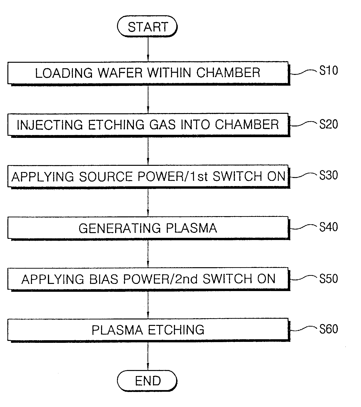
[0034]Hereinafter, preferred embodiments of the present invention will be described in detail.

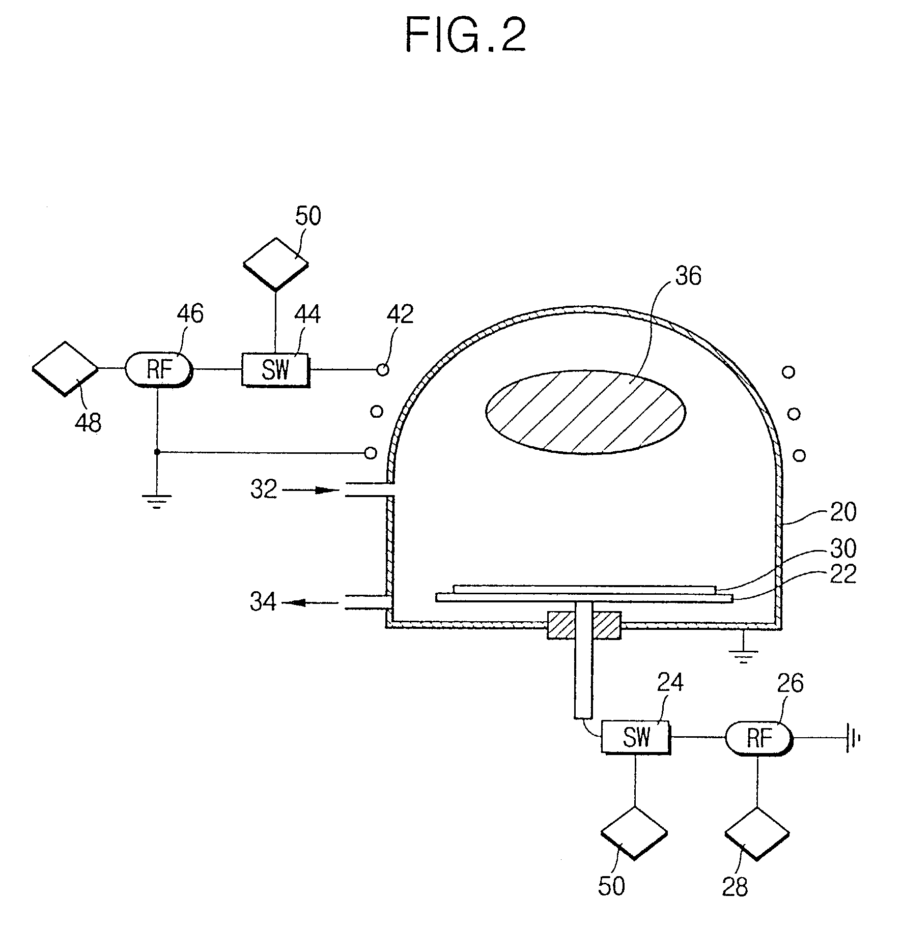
[0035]FIG. 2 is a schematic cross-sectional view of a decoupled plasma apparatus for implementing a dry etching process.

[0036]A decoupled plasma apparatus mainly includes a chamber 20 which is earth grounded, a first generator for providing a source power 46 for generating a magnetic field in the chamber 20 of RF (radio frequency) to produce plasma, a source power controller 48 for controlling an application or not, an intensity, an applying time, etc. of the source power 46, a second generator for providing a bias power 26 for generating an electric field of RF to impart a directional characteristic to thus produced ions of the plasma and a bias power controller 28 for controlling an application or not, an intensity, an applying time, etc. of the bias power 26.

[0037]A first switch for the source power 44 is turned on to supply the source power 46 to a coil 42 that wraps a dome-shaped upper...


PUM


Abstract

Disclosed is an etching method for semiconductor processing by which a pattern loading phenomenon is reduced. First, plasma is generated while setting a bias power applied to a wafer to zero and applying a source power. After a predetermined time period, an etching process is implemented onto a predetermined layer formed on the wafer by setting the bias power to a predetermined value. Since by-products generated during preceding etching processes can be readily removed during an etching using plasma, an etching process change due to a difference of pattern densities can be reduced. In addition, a progressive pattern loading generated as the number of processed wafers increase, can be prevented.

Description

BACKGROUND OF THE INVENTION[0001]1. Field of the Invention[0002]The present invention relates generally to an etching method in semiconductor processing and an etching system for performing the same, and more particularly, to an etching method in semiconductor processing for reducing a pattern loading phenomenon occurring at regions of a semiconductor device during plasma-based dry etching.[0003]2. Description of the Related Art[0004]Recently, the design of devices utilizing semiconductors has progressed rapidly due to the wide spread use of information media such as personal computers, mobile devices, mobile phones, etc. In turn, this rapid progression has demanded semiconductor devices to function at high operating speeds and to have large storage capacities. In order to satisfy such requirements, semiconductor devices with increased integration, reliability, and response time are aggressively being developed. To accomplish a highly integrated device, a reduction of a memory cell ...

Claims


Application Information

Patent Timeline
Patent Type & Authority Patents(United States)
IPC IPC(8): H01L21/461H01L21/302H01L21/3065H01L21/28H01L21/311H01L21/3213
CPCH01J37/321H01L21/32137H01L21/32136H01L21/31116H01L21/28123H01L21/3065
Inventor JUNG, YOUNG-JAE
Owner CONVERSANT INTPROP MANAGEMENT INC
Why Eureka
Try Eureka