Touch sensor, display device, and electronic apparatus

a display device and touch sensor technology, applied in the field of touch sensor, display device, electronic apparatus, can solve the problems of limiting the location where the conductive film can be disposed, the inability to dispose of the conductive film in a deeper portion of the liquid crystal, and the difficulty of using such a liquid crystal device display element for mobile apparatus applications, etc., to achieve the effect of reducing the influence of nois

Active Publication Date: 2014-10-14
JAPAN DISPLAY INC
View PDF9 Cites 18 Cited by
  • Summary
  • Abstract
  • Description
  • Claims
  • Application Information

AI Technical Summary

Benefits of technology

[0007]Accordingly, a conceivable solution would be to provide, in addition to a common electrode originally provided for applying a display drive voltage, a touch detection electrode that forms an electrostatic capacitance between the common electrode and the touch detection electrode (a display device including a capacitive touch sensor of a novel structure). That is, since this electrostatic capacitance changes depending on the presence / absence of contact or proximity of an object, if a display drive voltage applied to the common electrode by a display control circuit is also used (doubled) as a touch sensor drive signal, a detection signal responsive to a change in electrostatic capacitance is obtained from the touch detection electrode. Then, if this detection signal is inputted to a predetermined touch detection circuit, it is possible to detect the presence / absence of contact or proximity of an object. In addition, according to this technique, it is possible to obtain a display device with a touch sensor which can be even adapted for mobile apparatus applications in which the electric potential on the user side is often inconstant. Further, there are also advantages in that it is possible to obtain a display device with a touch sensor having a high degree of design freedom in accordance with the type of display function layer, and integration of circuits for display and circuits for sensor on a single circuit board is also facilitated, allowing for easy circuit integration.
[0009]Accordingly, to prevent erroneous operation (erroneous detection) due to noise resulting from the image signal writing operation, according to U.S. Pat. No. 6,057,903 and Japanese Unexamined Patent Application Publication (Translation of PCT Application) No. 56-500230 mentioned above, a transparent conductive layer (shield layer) is provided between the touch sensor and the display element. Then, by fixing this conductive layer to a constant potential, it is possible to shield against the above-mentioned noise from the display element.
[0013]It is desirable to provide a capacitive touch sensor that makes it possible to improve the accuracy of object detection, and a display device and an electronic apparatus including such a touch sensor.

Problems solved by technology

Therefore, aside from stationary television receivers which draw power from a socket, realistically, it is difficult to use such a liquid crystal device display element for mobile apparatus applications.
In addition, according to the technique mentioned above, since it is necessary that the conductive film for touch sensor be located very close to the user's finger, there are limits to the location where the conductive film can be disposed, such that it is not possible to dispose the conductive film in a deeper portion of the liquid crystal display element, for example.
That is, the degree of freedom of design is small.
Further, the configuration according to the above-mentioned technique makes it necessary to provide circuit portions such as a touch sensor drive portion and a coordinate detecting portion separately from a display drive circuit portion for the liquid crystal display element, making it difficult to achieve circuit integration for the apparatus as a whole.
The problem with capacitive touch sensors, including those according to Japanese Unexamined Patent Application Publication No. 2008-9750, U.S. Pat. No. 6,057,903, and Japanese Unexamined Patent Application Publication (Translation of PCT Application) No. 56-500230 mentioned above, and the above-mentioned novel structure, is that when writing a pixel signal (image signal) to the display element at each pixel, noise (internal noise) resulting from the writing operation is added to the detection signal.

Method used


Image

  • Touch sensor, display device, and electronic apparatus
  • Touch sensor, display device, and electronic apparatus
  • Touch sensor, display device, and electronic apparatus

Examples


first embodiment (

1. First Embodiment (an example of internal noise removal method using two drive lines of different widths)

second embodiment (

2. Second Embodiment (an example using a liquid crystal element of a transverse electric field mode as a display element)

3. Applications (applications of a display device with a touch sensor to an electronic apparatus)

4. Other Modifications

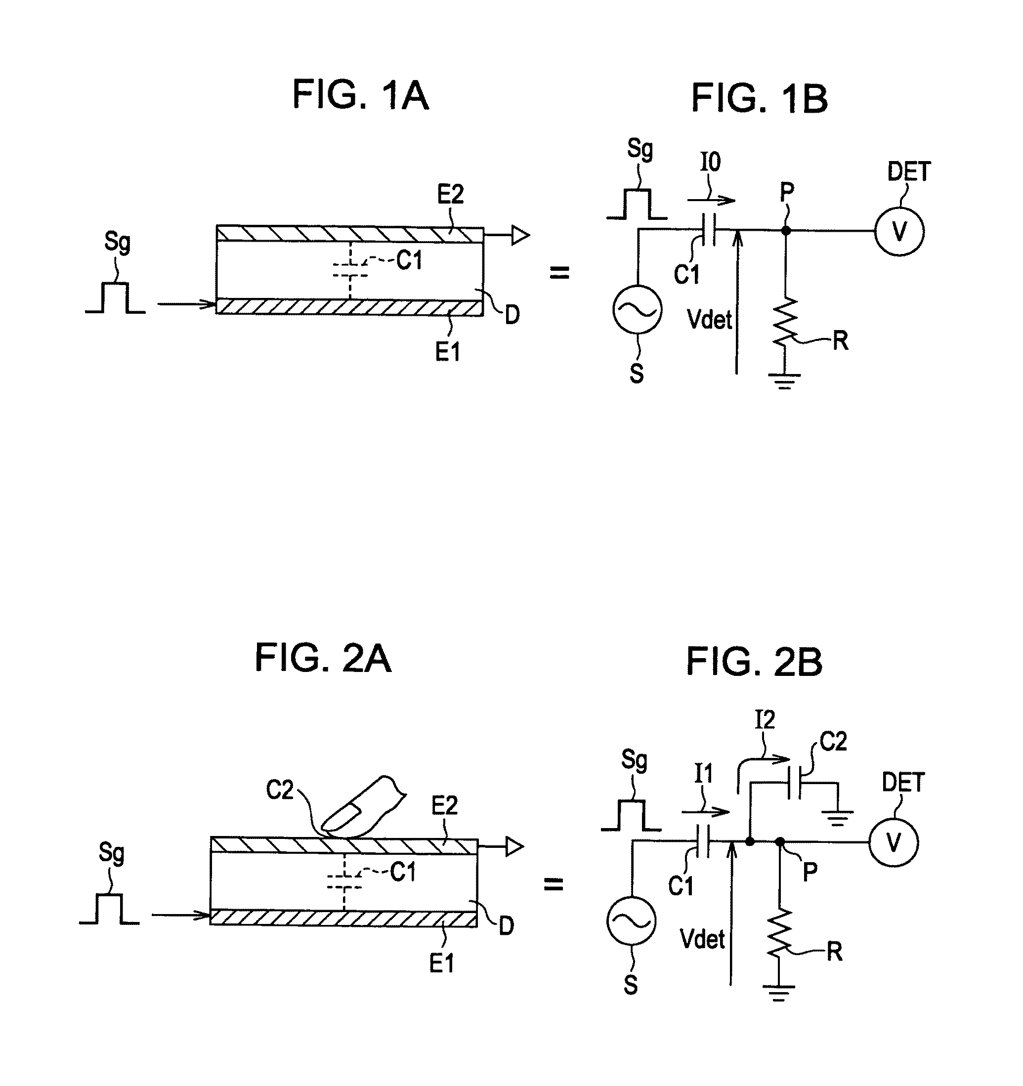
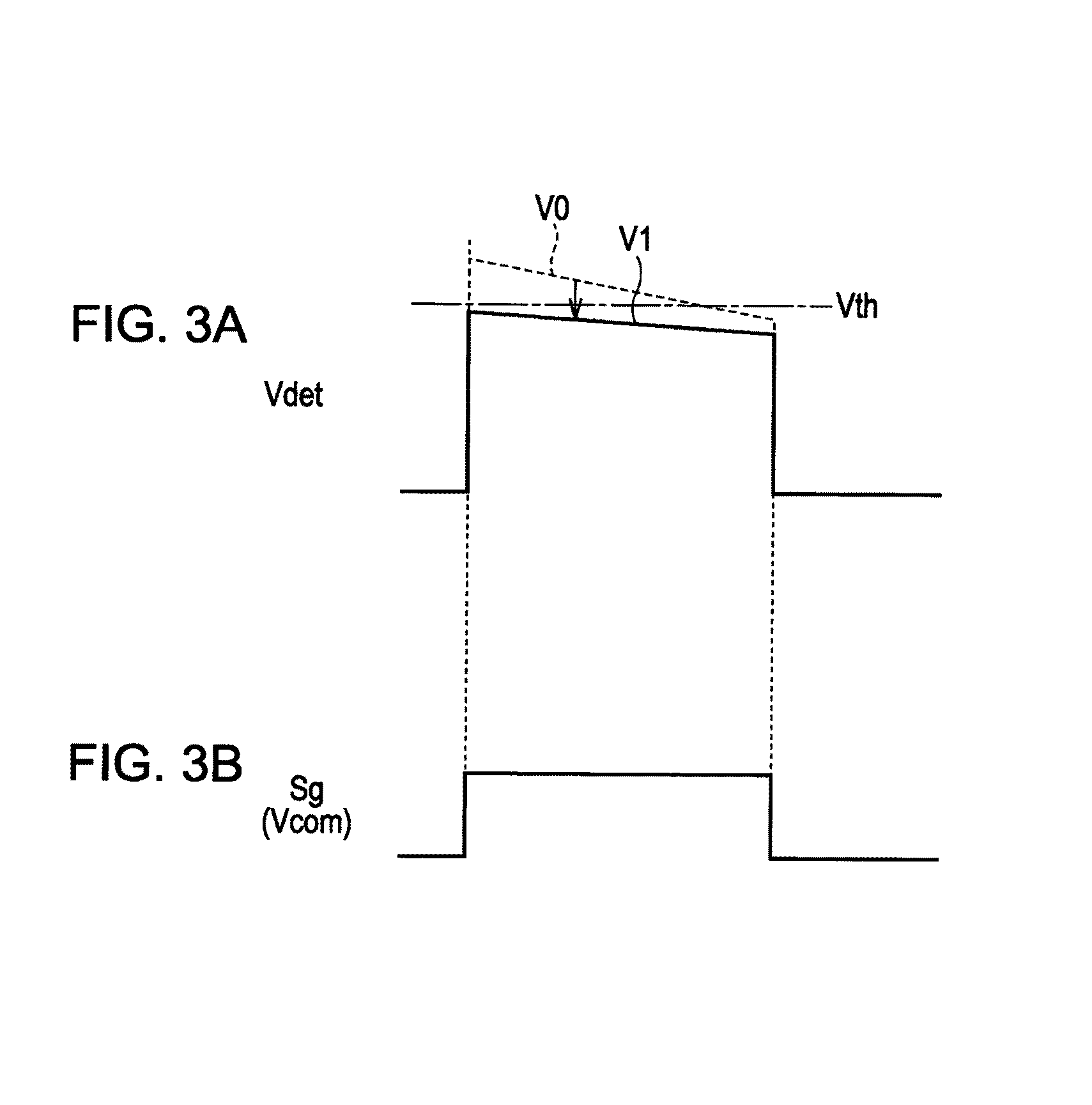
[0049]First, referring to FIGS. 1A to 3B, a description will be given of the basic principle of a touch detection system in a display device with a touch sensor according to an embodiment of the present invention. This touch detection system is to be implemented as a capacitive touch sensor. For example, as shown in FIG. 1A, a capacitor is formed by using a pair of electrodes (a drive electrode E1 and a detection electrode E2) opposed to each other with a dielectric D therebetween. This structure is represented as an equivalent circuit shown in FIG. 1B. A capacitor C1 is formed by the drive electrode E1, the detection electrode E2, and the dielectric D. One end of the capacitor C1 is connected to an AC signal source (drive signal source) S, and th...

first embodiment

1. First Embodiment

Example of Configuration of Display Device 1

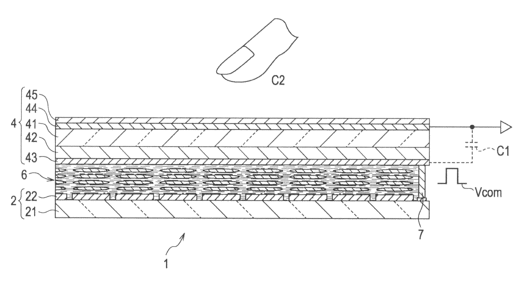
[0052]FIG. 4 shows the cross-sectional structure of the main portion of a display device 1 with a touch sensor according to a first embodiment of the present invention. In the display device 1, a capacitive touch sensor is formed by using a liquid crystal display element as a display element, and sharing the use of part (common electrode 43 described later) of electrodes originally provided to this liquid crystal display element and a display drive signal (common drive signal Vcom described later).

[0053]As shown in FIG. 4, the display device 1 includes a pixel substrate 2, a counter substrate 4 opposed to the pixel substrate 2, and a liquid crystal layer 6 inserted between the pixel substrate 2 and the counter substrate 4.

[0054]The pixel substrate 2 has a TFT substrate 21 as a circuit board, and a plurality of pixel electrodes 22 disposed in matrix on the TFT substrate 21. In addition to display drivers and TFTs (thin fi...


PUM


Abstract

A touch sensor includes a touch drive electrode, a touch detection electrode provided opposed to or side by side with the touch drive electrode and forming an electrostatic capacitance between the touch detection electrode and the touch drive electrode, and a touch detection circuit detecting a contact or proximity position of an object on the basis of a detection signal obtained from the touch detection electrode by applying a touch sensor drive signal to the touch drive electrode. The touch drive electrode is split into plural stripe-like electrode patterns. Applying the touch sensor drive signal to part of the electrode patterns forms a drive line at that time. The touch detection circuit performs a detection on the basis of a first detection signal obtained from a first drive line formed in a first period, and a second detection signal obtained from a second drive line formed in a second period.

Description

BACKGROUND OF THE INVENTION[0001]1. Field of the Invention[0002]The present invention relates to a display device such as a liquid crystal display device, in particular, a capacitive touch sensor that allows a user to input information by bringing a finger or the like into contact with or proximity to the touch sensor, and a display device and an electronic apparatus including such a touch sensor.[0003]2. Description of the Related Art[0004]Recently, attention has been paid to a type of display device which has a contact detecting device (hereinafter, referred to as touch sensor) or a so-called touch panel directly mounted on a liquid crystal display device, and in which various buttons are displayed on the liquid crystal display device instead of ordinary buttons to allow input of information. Since this technology enables shared placement of the display and buttons amid the growing tendency toward larger screen sizes of mobile apparatus, the technology provides significant advanta...

Claims


Application Information

Patent Timeline
Patent Type & Authority Patents(United States)
IPC IPC(8): G06F3/045G06F3/041G06F3/044
CPCG06F3/0412G06F3/044G06F3/0418G06F1/1643G06F3/0416G06F3/04166G06F3/0445G06F3/0446
Inventor TAKEUCHI, TAKEYANOGUCHI, KOJIISHIZAKI, KOJINAKANISHI, TAKAYUKITERANISHI, YASUYUKI
Owner JAPAN DISPLAY INC
Why Eureka
Try Eureka