Multilevel interconnection system

a multi-level, interconnection technology, applied in the direction of coupling device connection, association of printed circuit parts, printed circuit non-printed electric components, etc., can solve the problems of bare chip that is increasingly shrinking in size, conventional connection techniques do not allow to provide a sufficient number of contacts, etc., to prevent erroneous connection of male and female connection components, simple and reliable production, and reliable shape coding

Active Publication Date: 2014-11-18
VLSI TECH LLC
View PDF27 Cites 19 Cited by
  • Summary
  • Abstract
  • Description
  • Claims
  • Application Information

AI Technical Summary

Benefits of technology

[0016]The term “chip package” may particularly denote a housing that chips come in for plugging into (socket mount) or soldering onto (surface mount) a circuit board such as a printed circuit board, thus creating a mounting for a chip. In electronics, the term chip package or chip carrier may denote the material added around a component or integrated circuit to allow it to be handled without damage and incorporated into a circuit.
[0044]Furthermore, by a corresponding or matching shape of the protrusion and the recess, a shape coding feature may be implemented which allows to connect the male connection component with the female connection component so that an erroneous connection may be avoided.

Problems solved by technology

The ability to provide more and more I / O interconnections to a die (bare chip) that is increasingly shrinking in size is an important issue.
In addition, the smaller size of the package contributes as much to the miniaturization of cellphones and other handheld devices as the shrinking of the semiconductor circuits.
However, conventional connection techniques do not allow to provide a sufficient number of contacts when pieces to be connected become smaller and smaller.

Method used


Image

  • Multilevel interconnection system
  • Multilevel interconnection system
  • Multilevel interconnection system

Examples


Embodiment Construction

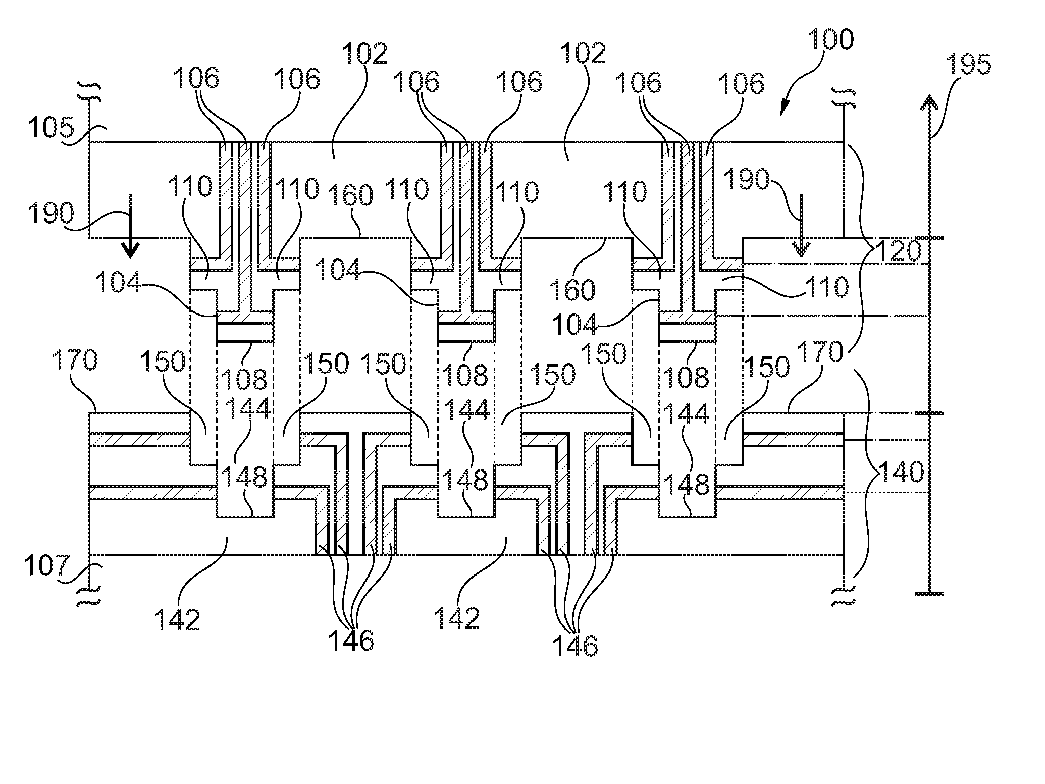
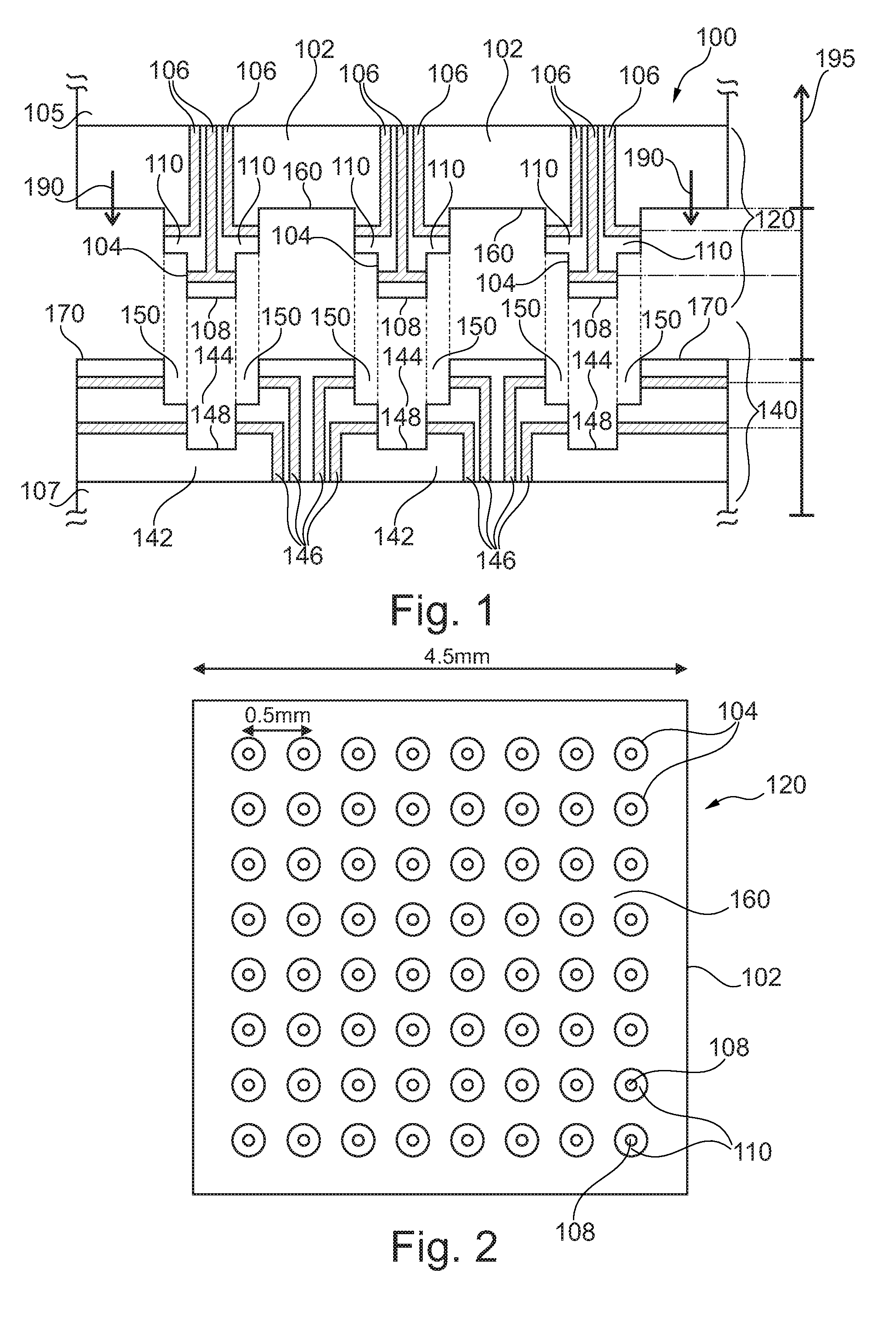
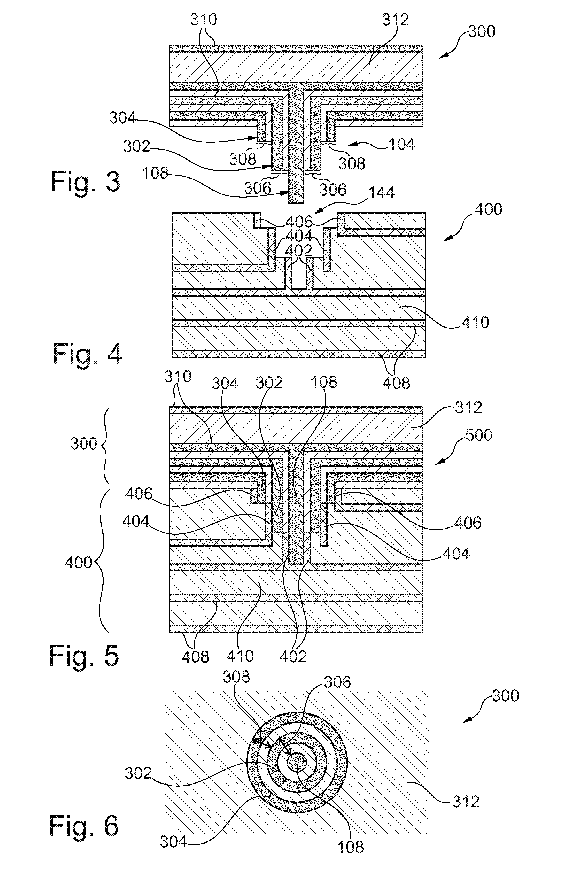
[0057]The illustration in the drawing is schematically. In different drawings, similar or identical elements are provided with the same reference signs.

[0058]In the following, such basic recognitions of the present inventor will be mentioned based on which exemplary embodiments of the invention have been developed.

[0059]Nowadays semiconductors manufacturers do apply BGA (ball grid array), QFN (Quad Flat No-Lead) and other leaded and leadless packages to provide a connectable semiconductor device to a system integrator (like a handheld manufacturer) who usually solders (or glues) the leads or contacts of the package, which are distributed two-dimensionally on the package, on a printed circuit board.

[0060]For WLCSP (wafer level chip scale packages), this two-dimensional arrangement of the interconnections (which can be bumps, leads, balls, etc.—herein shortly called bumps) restricts the maximum number of input / output connections (I / Os) on the WLCSP. The minimum bump size and the minim...


PUM

PropertyMeasurementUnit
sizeaaaaaaaaaa
sizeaaaaaaaaaa
side lengthaaaaaaaaaa

Abstract

A male connection component (120) for connection with a correspondingly configured female connection component (140) having a recess (144) extending into a main surface (170) of a female Substrate (142) of the female connection component (140), wherein the female connection component (140) comprises a plurality of electrically conductive female contacts (146) which are electrically decoupled from one another and are arranged at different height levels with regard to the main surface (170) of the female Substrate (142), the male connection component (120) comprising a male Substrate (102), a Protrusion (104) protruding from a main surface (160) of the male Substrate (102) and comprising a plurality of electrically conductive male contacts (106) which are electrically decoupled from one another and are arranged at different height levels with regard to the main surface (160) of the male Substrate (102), wherein the male connection component (120) is adapted for connection with the female connection component (140) so that upon connection, each of the plurality of electrically conductive male contacts (106) is brought in contact with one of the plurality of electrically conductive female contacts (146) for providing electric contactation at different height levels, wherein the male Substrate (102) forms at least part of one of a chip, a chip package and a circuit board.

Description

FIELD OF THE INVENTION[0001]The invention relates to a male connection component.[0002]The invention further relates to a female connection component.[0003]Moreover, the invention relates to an electronic apparatus.[0004]Furthermore, the invention relates to a method of connecting a male connection component with a female connection component.BACKGROUND OF THE INVENTION[0005]For instance for packaging semiconductor chips and for connecting the packaged semiconductor chip to a printed circuit board, a number of electric contacts has to be made. The ability to provide more and more I / O interconnections to a die (bare chip) that is increasingly shrinking in size is an important issue. In addition, the smaller size of the package contributes as much to the miniaturization of cellphones and other handheld devices as the shrinking of the semiconductor circuits.[0006]WO 02 / 13253 discloses a method of producing a female microconnector for connection to a microcomponent having a correspondin...

Claims


Application Information

Patent Timeline
Patent Type & Authority Patents(United States)
IPC IPC(8): H01R103/00H05K1/02H01L23/498H05K1/18H01R24/40H01L23/00H01R24/38H01R12/00
CPCH01R24/40H01L2924/00H01L24/81H01L24/72H01L2924/01082H01L2924/01076H01L2924/00011H05K2201/09036H01L24/10H05K2201/092H01L2224/16237H05K1/184H05K2201/09809H01L2924/01015H01L24/90H01L2924/01033H01L2924/01005H05K2201/09845H01L24/13H01L24/16H01L2924/3512H01L2924/10253H01L2224/05578H01L2924/014H01L2924/14H01L2224/13078H01L2224/13099H01L2224/83136H01L2224/83851H05K1/0243H01R23/26H01L2924/01023H01L2924/01032H01L24/83H01L2924/01029H01R2103/00H05K1/0298H01L2224/90H01L23/49811H01L2223/6622Y10T29/49117H01L2224/16235H01L2224/0401H01L2224/81898H01L2224/13H01L2224/16106H01L2224/06131H01L2224/16105H01R24/00
Inventor PISCHLER, ERICH
Owner VLSI TECH LLC
Why Eureka
Try Eureka