CMOS differential logic circuit using voltage boosting technique

a technology of differential logic and voltage boosting, which is applied in logic circuits, pulse techniques, reliability increasing modifications, etc., can solve the problems of extreme voltage scaling that is not acceptable, the operating speed of the transistor is greatly reduced, and the approach is limited to use, so as to improve the energy efficiency of high-speed operation and prevent the effect of reducing the operating speed

Active Publication Date: 2014-12-09
RES & BUSINESS FOUND SUNGKYUNKWAN UNIV
View PDF6 Cites 5 Cited by
  • Summary
  • Abstract
  • Description
  • Claims
  • Application Information

AI Technical Summary

Benefits of technology

[0032]Accordingly, the present invention has been made in an effort to solve the problems occurring in the related art and an object of the present invention is to provide a CMOS differential logic circuit using a voltage boosting technique which is capable of preventing reduction in operating speed by outputting voltage higher than source voltage even in a low-source-voltage environment according to a capacitive-coupling-based boosting technique and improving energy efficiency for high-speed operation by using only one bootstrapped capacitor.
[0040]The voltage-boosting unit reduces the delay time attributable to the low source voltage by increasing the voltage at the second node NP by the boosting voltage.
[0041]The voltage-boosting unit increases the load driving abilities of the first and second inverter drivers by increasing the inter-electrode voltages of second switching elements included in the first and second inverter drivers.

Problems solved by technology

This approach is limited to use only in low-end designs in which operating speed is a secondary concern because of severe speed degradation, attributable to the low switching current, and great performance variability due to changes in process, temperature, and threshold voltage.
In contrast, for medium- and high-end circuits, where both speed performance and energy efficiency are important, extreme voltage scaling is not acceptable, and instead, a near-threshold voltage design is more suitable for achieving relatively high energy efficiency without severe speed degradation.
As a result, the operating speed of the transistor is greatly reduced.
The conventional DCVS circuit, however, is problematic in that, like the existing CMOS logic, the operating speed is greatly reduced when the source voltage VDD is scaled down because the output current is proportional to the supplied source voltage VDD.
However, since the circuit is used as a large capacitive-load driver, logic functions cannot be efficiently embedded into the circuit.
As described above, since the conventional BDL circuit must use two large-capacitive bootstrapped capacitors, the operating speed of this logic style is not improved much due to the addition of the overall latency of the circuit.
In addition, although some recent circuit techniques adopting bootstrapped operation have been proposed, they are not all for logic composition.
Accordingly, there is a problem in that energy consumption is also increased in proportion thereto.
When the source voltage VDD is scaled down, however, there is a problem in that the operating speed of the system is reduced because the operating speed of the transistor is sharply reduced.

Method used


Image

  • CMOS differential logic circuit using voltage boosting technique
  • CMOS differential logic circuit using voltage boosting technique
  • CMOS differential logic circuit using voltage boosting technique

Examples


Embodiment Construction

[0054]Reference will now be made in greater detail to a preferred embodiment of the invention, an example of which is illustrated in the accompanying drawings. Wherever possible, the same reference numerals will be used throughout the drawings and the description to refer to the same or like parts.

[0055]An exemplary embodiment of a CMOS differential logic circuit using a voltage boosting technique (BCDL) in accordance with the present invention is described below with reference to the accompanying drawings.

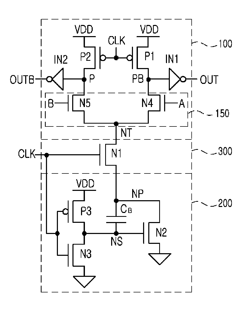
[0056]FIG. 3 is a circuit diagram of a CMOS differential logic circuit using a voltage boosting technique in accordance with the present invention. The CMOS differential logic circuit includes a precharge differential logic unit 100, a voltage-boosting unit 200, and a switching unit 300.

[0057]The precharge differential logic unit 100 includes first and second PMOS transistors P1 and P2, a differential logic tree 150, and first and second inverter drivers IN1 and IN2. The different...


PUM


Abstract

The present invention discloses a CMOS differential logic circuit. The CMOS differential logic circuit includes a precharge differential logic unit, which is precharged to a source voltage in response to a clock signal and is configured to output voltage having an increased load-driving ability using a boosting voltage; a voltage-boosting unit, which is pulled down by a ground voltage in response to the clock signal and is configured to boost the pulled-down voltage using capacitive coupling and output the boosting voltage; and a switching unit, which is configured to couple the precharge differential logic unit and the voltage-boosting unit in response to the clock signal. The propagation delay of a signal from the input terminal to the output terminal of a circuit in a low-source-voltage environment can be reduced, and the operating speed of the circuit and energy efficiency of the operation thereof can be improved.

Description

CROSS-REFERENCE TO RELATED APPLICATION[0001]This application claims the benefit under 35 U.S.C. §119(a) of Korean Patent Application No. 10-2012-0139895, filed on Dec. 4, 2012, in the Korean Intellectual Property Office, the entire disclosure of which is incorporated herein by reference for all purposes.BACKGROUND[0002]1. Field[0003]The present invention relates to a CMOS differential logic circuit, and more particularly, to a CMOS differential logic circuit using a voltage boosting technique, which is capable of improving operating speed and energy efficiency in a low-source-voltage environment in such a way as to supply a source voltage boosted by the capacitive coupling of a MOS transistor for transferring a signal from an input terminal to an output terminal.[0004]2. Description of the Related Art[0005]The increasing interest in energy-efficient design is provoking a growing need for portable devices that consume energy efficiently.[0006]Since most energy consumption of modern d...

Claims


Application Information

Patent Timeline
Patent Type & Authority Patents(United States)
IPC IPC(8): H03K17/16H03K19/096H03K19/0185
CPCH03K19/018528H03K19/0948
Inventor KONG, BAI SUNKIM, JONG WOOKIM, JOO SEONG
Owner RES & BUSINESS FOUND SUNGKYUNKWAN UNIV
Why Eureka
Try Eureka