


Quick Research
Generate reliable direction feasibility study reports for your R&D in just a few steps.

Technical Q&A
Discover and master advanced knowledge NOW. Basics, ideas, possibilities, all at once.

Find Solutions
As an expert in R&D theories, this can generate solutions to your technical problems instantly.

Evaluate Feasibility
Analyze your overall solution with one click, know your potential R&D risks in advance.

Monitor Landscape
Get weekly tech updates, stay abreast of the latest tech innovations and key insights.
Materials for organic electroluminescence device
- Summary
- Abstract
- Description
- Claims
- Application Information
AI Technical Summary
Benefits of technology
Problems solved by technology
Method used
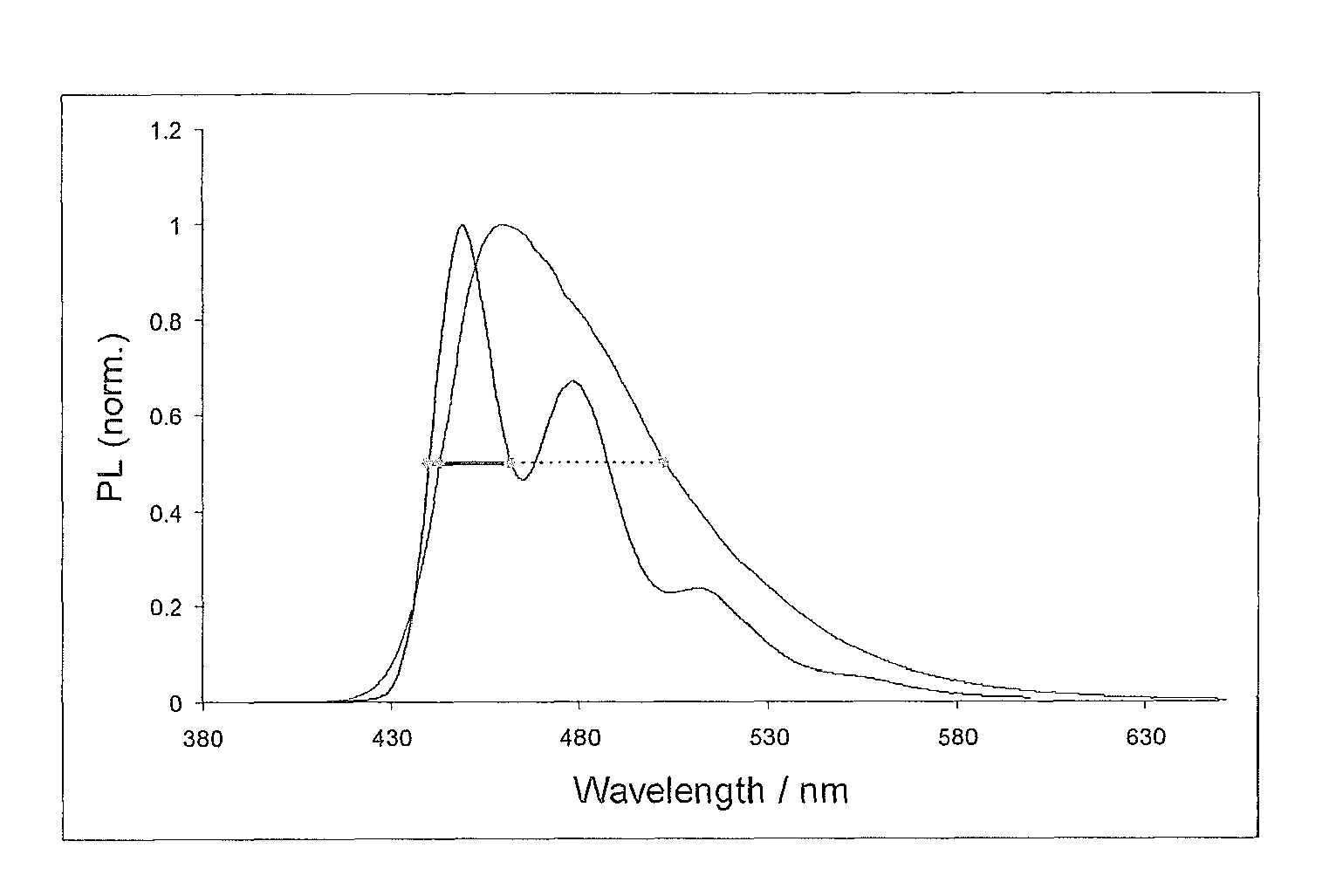
Image

Examples
example 1
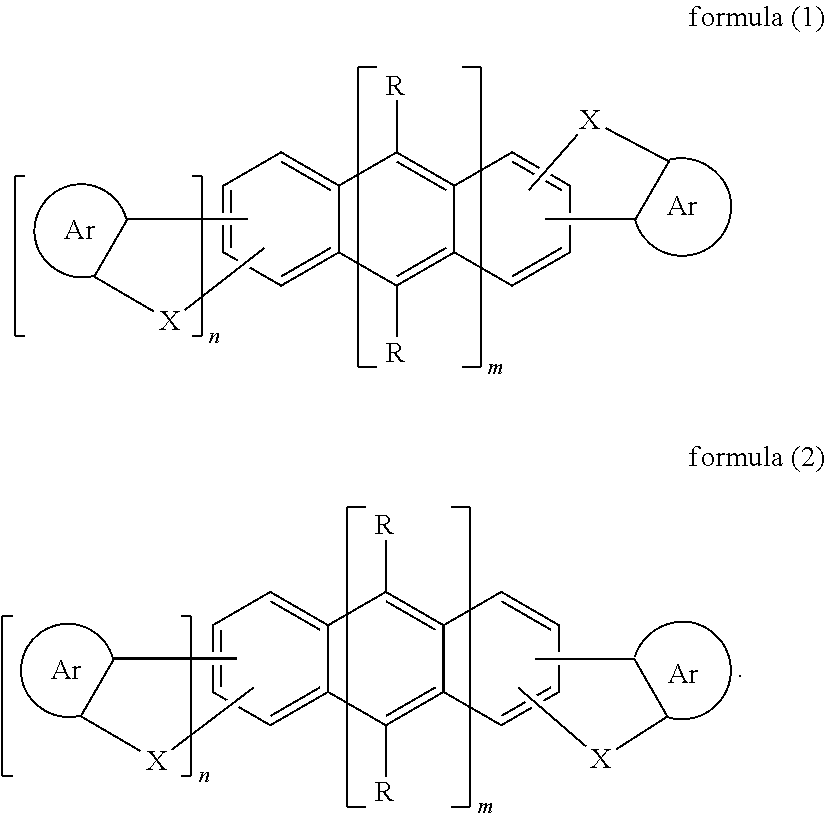
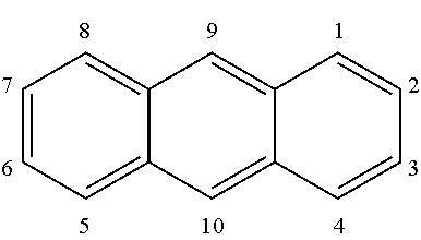
2,3,8,9-Dibenzo-1,1,7,7-tetraphenyl-5,11-diphenyl-1,7-dihydrodicyclopenta[b,i]anthracene
a) Synthesis of 2,6-dibromoanthraquinone
[0102](Lee et al., Organic Letters 2005, 7(2), 323-326)
[0103]
[0104]62.6 g (255 mmol) of 2,6-diaminoanthraquinone and 124 g (550 mmol) of CuBr2 are initially introduced in 1000 ml of acetonitrile, and 68 ml (515 mmol) of tert-butyl nitrite are added dropwise at an internal temperature of 60° C. After 30 min., the reaction mixture is poured into a mixture of 150 ml of concentrated HCl and 1 l of ice-water, and the solid formed is filtered off with suction, washed with water, EtOH and heptane and dried, giving 89 g (243 mmol, 96%) of a brown solid, which is homogeneous in the 1H-NMR and which is employed in the subsequent reaction without further purification.
b) Synthesis of 2,6-dibromo-9,10-diphenylanthracene
[0105]
[0106]36.6 g (100 mmol) of 2,6-dibromoanthraquinone are dissolved in 600 ml of THF, the solution is cooled to −75° C., and 100 ml of a 2 M phenylli...
example 2
2,3-Benzo-1,1-diphenyl-5,11-diphenyl-1-dihydrocyclopenta[b]anthracene
[0115]
[0116]The synthesis of this compound is carried out analogously to Example 1, with 2-aminoanthraquinone being employed as starting compound.
example 3
Production of OLEDs
[0117]OLEDs are produced by a process which is described in general terms in WO 04 / 058911 and which is adapted in individual cases to the respective circumstances (for example layer-thickness variation in order to achieve optimum efficiency or colour).
[0118]The results for various OLEDs are presented in Examples 4 to 7 below. Glass plates which are coated with structured ITO (indium tin oxide) form the substrates of the OLEDs. The OLEDs consist of the following layer sequence: substrate / hole-injection layer (HTM1) 60 nm / hole-transport layer (HTM2) 20 nm / emission layer (EML) 30 nm / electron-transport layer (ETM) 20 nm and finally a cathode. The materials are vapour-deposited thermally in a vacuum chamber. The emission layer here always consists of a matrix material (host) and a dopant, which is admixed with the host by co-evaporation. The cathode is formed by a 1 nm thin LiF layer and a 100 nm Al layer deposited on top.
[0119]Table 1 shows the chemical structures of ...
PUM
| Property | Measurement | Unit |
|---|---|---|
| Fraction | aaaaa | aaaaa |
| Fraction | aaaaa | aaaaa |
| Electric potential / voltage | aaaaa | aaaaa |
Abstract
Description
Claims
Application Information
 - R&D Engineer
- R&D Manager
- IP Professional
- Industry Leading Data Capabilities
- Powerful AI technology
- Patent DNA Extraction
Browse by: Latest US Patents, China's latest patents, Technical Efficacy Thesaurus, Application Domain, Technology Topic, Popular Technical Reports.
© 2024 PatSnap. All rights reserved.Legal|Privacy policy|Modern Slavery Act Transparency Statement|Sitemap|About US| Contact US: help@patsnap.com