Signal processing circuit

a technology of signal processing and circuit, applied in the field of signal processing circuit, can solve the problems of limited number of rewrite cycles, significant deterioration of memory elements, and writing errors, and achieve the effects of reducing writing errors and reading errors, low power consumption, and high reliability

Inactive Publication Date: 2015-01-06
SEMICON ENERGY LAB CO LTD
View PDF125 Cites 6 Cited by
  • Summary
  • Abstract
  • Description
  • Claims
  • Application Information

AI Technical Summary

Benefits of technology

[0017]In such a nonvolatile storage circuit, the transistor with extremely low off-state current is turned on by inputting a second high power supply potential to the gate of the transistor. Here, the second high power supply potential is higher than the first high power supply potential. For example, (the second high power supply potential)>(the first high power supply potential)+Vth is set, where Vth is the threshold voltage of the transistor with extremely low off-state current. Then, a predetermined potential is input to the retention node through the transistor in the on state. After that, the transistor is turned off by inputting the ground potential (0 V, corresponding to the low power supply potential) to the gate of the transistor, and the predetermined potential is held. Note that the transistor with extremely low off-state current is an enhancement-mode (normally-off) n-channel transistor. When supply of the power supply voltage to the whole signal processing circuit or some circuits included in the signal processing circuit is stopped, the ground potential (0 V) continues to be input to the gate of the transistor. For example, the gate of the transistor is grounded through a load such as a resistor. Accordingly, the transistor can be kept off even after supply of the power supply voltage to the whole signal processing circuit or some circuits included in the signal processing circuit is stopped; thus, the potential of the retention node can be held for a long time.
[0041]One of features of the present invention is that a potential input to a gate of a transistor with extremely low off-state current to turn on the transistor is higher than a potential input to a source or a drain of the transistor, for example, by the threshold voltage of the transistor, and thus a signal potential can be precisely transmitted through the transistor. Therefore, the present invention is not limited to a signal processing circuit and is applicable to any semiconductor device including a transistor having the following structure: a potential input to its gate to turn it on is higher than a potential input to its source or drain, for example, by the threshold voltage. The use of such a transistor makes it possible to increase the quality of a semiconductor device. For example, the present invention can be a display device including the transistor in each pixel. Examples of a display device are a liquid crystal display device and an electroluminescent display device. That is, the transistor may be used as a transistor for controlling input of a signal voltage to a liquid crystal element or an electroluminescent element; thus, a display device with high display quality can be provided. For example, the present invention can be a storage device including the transistor in a memory cell, and a highly reliable storage device can be provided as a result. Furthermore, the present invention can be, for instance, an image sensor and a touch panel that include the transistor in each pixel for taking images. Thus, a highly reliable image sensor and a highly reliable touch panel can be provided.

Problems solved by technology

In the memory element containing a ferroelectric, a ferroelectric material is fatigued by repetition of data writing, which causes a problem such as a writing error.
As a result, the number of rewrite cycles is limited.
This leads to a problem such that memory elements deteriorate significantly by repeated data rewriting, and the number of rewrite cycles is therefore limited.

Method used


Image

  • Signal processing circuit
  • Signal processing circuit
  • Signal processing circuit

Examples


embodiment 1

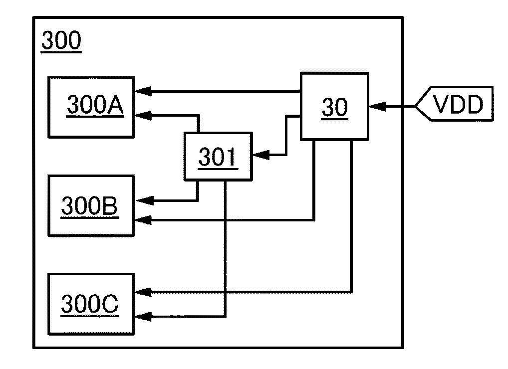
[0071]FIG. 1A illustrates a signal processing circuit according to one embodiment of the present invention. In FIG. 1A, a signal processing circuit 300 includes a circuit unit 300A, a circuit unit 300B, a circuit unit 300C, a power supply circuit 30, and a step-up circuit 301. A first high power supply potential (hereinafter also “VDD”) input to the signal processing circuit 300 is input to the power supply circuit 30. The power supply circuit 30 selectively supplies the first high power supply potential (VDD) to each of the circuit units (the circuit unit 300A, the circuit unit 300B, and the circuit unit 300C). Power consumption of the signal processing circuit can be reduced with a normally-off driving method by which the first high power supply potential (VDD), that is, the power supply voltage is selectively supplied only to a circuit unit intended to be operated. The power supply circuit 30 also supplies the first high power supply potential (VDD) to the step-up circuit 301. Th...

embodiment 2

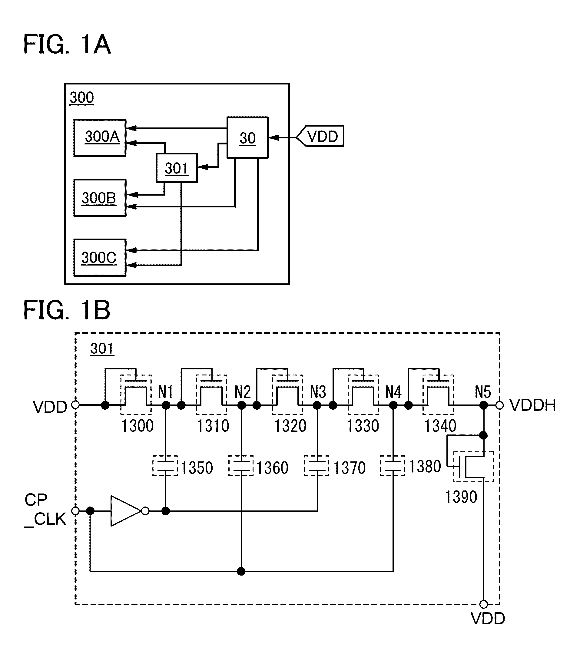
[0134]In this embodiment, one embodiment of the step-up circuit 301 in FIG. 1A of Embodiment 1 will be described.

[0135]FIG. 1B illustrates one embodiment of the step-up circuit 301. FIG. 1B illustrates an example of a four-stage step-up circuit. Typically, a step-up circuit performing n-stage step-up operations (n: a natural number) can be used. The first high power supply potential (VDD) is supplied to an input terminal (here, referring to a source terminal or a drain terminal that is electrically connected to a gate terminal) of a first transistor 1300. An output terminal (here, referring to the source terminal or the drain terminal that is not electrically connected to the gate terminal) of the first transistor 1300 is electrically connected to an input terminal of a second transistor 1310 and one of a pair of electrodes of a first capacitor 1350. Similarly, an output terminal of the second transistor 1310 is electrically connected to an input terminal of a third transistor 1320 ...

embodiment 3

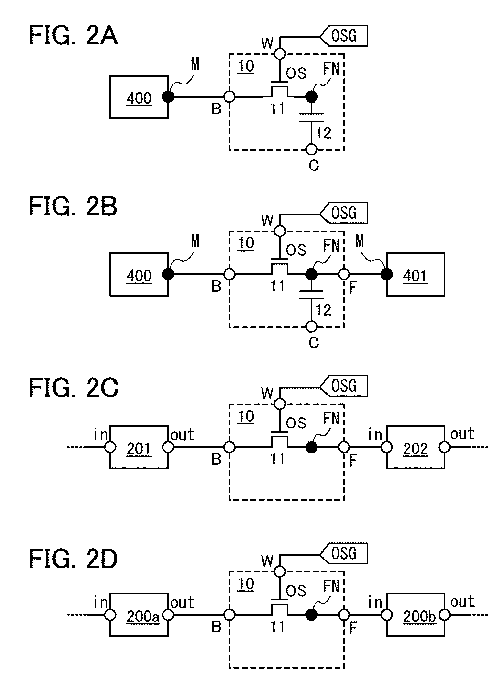
[0143]A method for manufacturing a signal processing circuit will be described. This embodiment explains a method for manufacturing a signal processing circuit, using the transistor 11 whose channel is formed in the oxide semiconductor layer, the capacitor 12, and a transistor 133 included in the arithmetic circuits 201 and 202 as an example of components included in the combination of the volatile storage circuit 200 and the nonvolatile storage circuit 10 illustrated in FIGS. 3A to 3E. Here, the case where a transistor whose channel is formed in a silicon layer is used as the transistor 133 is described as an example.

[0144]Note that the transistors (the first transistor 1300, the second transistor 1310, the third transistor 1320, the fourth transistor 1330, the fifth transistor 1340, and the transistor 1390 in FIG. 1B) included in the step-up circuit 301 can be formed in a manner similar to that of the transistor 11. Further, the capacitors (the first capacitor 1350, the second cap...


PUM


Abstract

A signal processing circuit including a nonvolatile storage circuit with a novel structure. The signal processing circuit includes a circuit that is supplied with a power supply voltage and has a first node to which a first high power supply potential is applied, and a nonvolatile storage circuit for holding a potential of the first node. The nonvolatile storage circuit includes a transistor whose channel is formed in an oxide semiconductor layer, and a second node that is brought into a floating state when the transistor is turned off. A second high power supply potential or a ground potential is input to a gate of the transistor. When the power supply voltage is not supplied, the ground potential is input to the gate of the transistor and the transistor is kept off. The second high power supply potential is higher than the first high power supply potential.

Description

BACKGROUND OF THE INVENTION[0001]1. Field of the Invention[0002]The present invention relates to a storage circuit that can keep a stored logic state even when power is off, and a storage device and a signal processing circuit that include the storage circuit. The present invention also relates to an electronic device including the storage circuit or the signal processing circuit.[0003]2. Description of the Related Art[0004]Signal processing circuits such as central processing units (CPUs) have a variety of configurations depending on their application and are generally provided with a variety of storage circuits such as a register and a cache memory as well as a main memory for storing data or a program.[0005]In a storage circuit such as a register or a cache memory, data needs to be read and written at higher speed than in a main memory. Thus, in general, a flip-flop is used as a register, and a static random access memory (SRAM) or the like is used as a cache memory. That is, a v...

Claims


Application Information

Patent Timeline
Patent Type & Authority Patents(United States)
IPC IPC(8): G11C7/00
CPCG11C7/00G11C11/404G11C16/0416H01L27/1225H10B41/70G11C5/063G11C16/06G11C16/30H10B69/00
Inventor MATSUZAKI, TAKANORI
Owner SEMICON ENERGY LAB CO LTD
Why Eureka
Try Eureka