Electrophotographic photoconductor, electrophotographic apparatus and process cartridge

a photoconductor and electrophotography technology, applied in the direction of electrographic process apparatus, corona discharge, instruments, etc., can solve the problems of limited improvement made on the resultant intermediate layer, increase in residual potential on the surface of the intermediate layer, and black spots on the image, etc., to achieve the effect of concealing pigments, increasing residual potential, and reducing the volume resistivity of the intermediate layer

Inactive Publication Date: 2015-01-13
RICOH KK
View PDF18 Cites 1 Cited by
  • Summary
  • Abstract
  • Description
  • Claims
  • Application Information

AI Technical Summary

Benefits of technology

[0026]The present invention aims to solve the existing problems and provide an electrophotographic photoconductor that changes in characteristics to a lesser extent even after repetitive use and involves increase in residual potential and formation of images with black spots to a lesser extent.
[0038]When the content of the titanium oxide in the inorganic pigment is less than 70% by mass, the impurities contained cause increase in residual potential during repetitive use. Whereas when it is more than 90% by mass, the volume resistivity of the intermediate layer considerably decreases, leading to degradation of image qualities during repetitive use to cause defects such as black spots or fogging. When the specific surface area is less than 70 m2 / g, dispersion treatment becomes easy but concealment of the pigment and the resin becomes poor, so that the volume resistivity of the intermediate layer decreases and abnormal images tend to be formed. Whereas when it is more than 140 m2 / g, the surface area of the inorganic pigment becomes large, so that the liquid viscosity tends to increase, making it difficult to attain a good dispersion state and stable production of an intermediate layer. When the volume ratio of the inorganic pigment in the intermediate layer is less than 30%, the volume resistivity of the intermediate layer increases to cause increase in residual potential. Whereas it is more than 50%, the intermediate layer becomes poor in coating qualities, resulting in reduction of adhesiveness to other layers. When the volume resistivity of the intermediate layer at an electrical field intensity of 2.5×10⁵ V / cm is less than 5×10¹¹ Ω·cm, abnormal current generated from the substrate causes defects such as black spots or fogging. Whereas when it is more than 1×10¹³ Ω·cm, the sensitivity decreases and the residual potential increases.
[0039]The present invention can provide an electrophotographic photoconductor that changes in characteristics to a lesser extent even after repetitive use and involves increase in residual potential and formation of images with black spots to a lesser extent. This electrophotographic photoconductor can solve the above existing problems.

Problems solved by technology

As a result, portions where charges are injected from the substrate into the photoconductive layer are not sufficiently charged to cause image defects such as black spots.
Meanwhile, when the electrical resistance of an intermediate layer is too high, the intermediate layer blocks positive and negative charges generated in a charge generation layer that are to be transferred to the substrate side upon exposure to light, leading to increase in residual potential on the surface of the intermediate layer.
This measure can overcome such disadvantages to some extent but when it is taken alone, improvements made on the resultant intermediate layer are limited.
Also, when a photoconductor is repeatedly used, charges trapped in its intermediate layer in a charging step causes delayed charging, in which the surface potential of the photoconductor does not increase right after charges are given to the photoconductor but normal charging starts after a certain amount of charges flows into the photoconductor.
Even when a photoconductor involving delayed charging is subjected to a charging process under such conditions as to provide a normal photoconductor with a sufficient charge potential, the surface potential of the photoconductor cannot reach a desired level before imagewise light exposure, so that unevenness in density of images disadvantageously occurs.
These methods can prevent increase in residual potential and formation of images with black spots but cause delayed charging due to repetitive use of the photoconductors.

Method used


Image

  • Electrophotographic photoconductor, electrophotographic apparatus and process cartridge
  • Electrophotographic photoconductor, electrophotographic apparatus and process cartridge
  • Electrophotographic photoconductor, electrophotographic apparatus and process cartridge

Examples


example 1

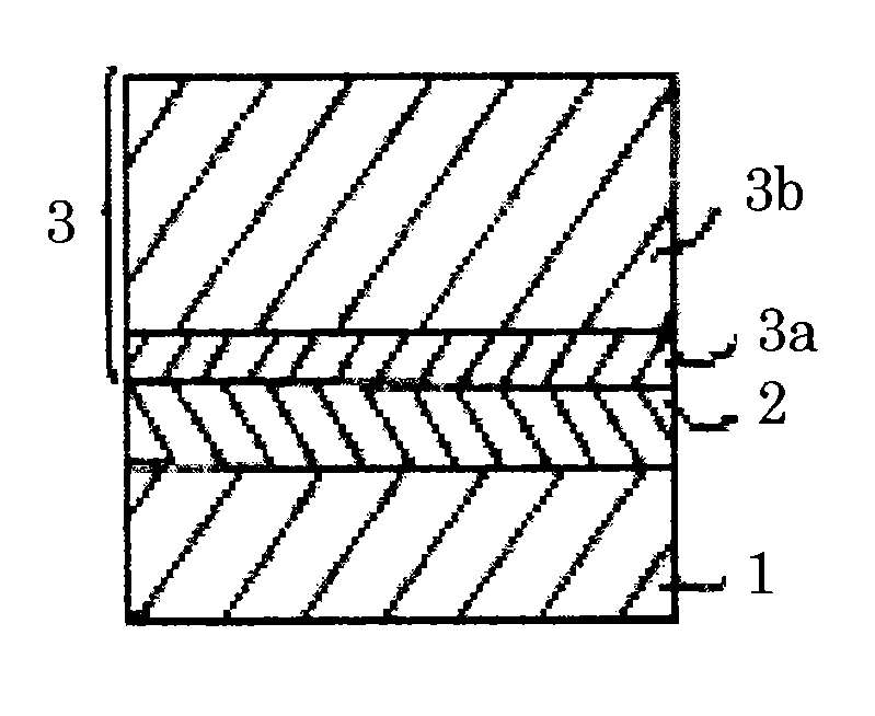
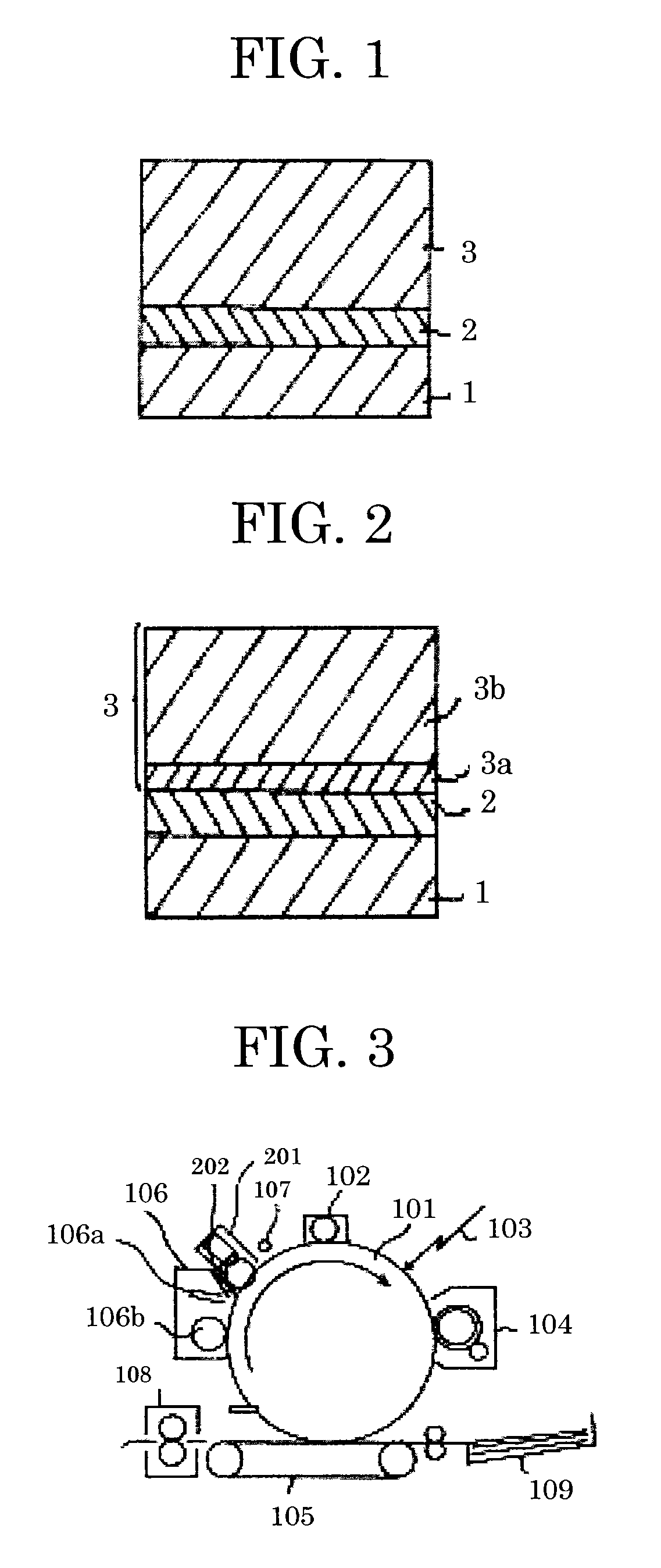
[0132]An electrophotographic photoconductor (photoconductor) of Example 1 was produced by sequentially forming an intermediate layer, a charge generation layer and a charge transport layer on an aluminum substrate according to the following procedure.

(Coating Liquid for an Intermediate Layer)

[0133]A 200 mL-mayonnaise bottle was charged with 18.7 parts of an inorganic pigment which is titanium oxide whose surface is treated with aluminum hydroxide (specific surface area: 85 m2 / g, content of titanium oxide: 83% by mass), 6.1 parts of a binder resin which is a polyamide copolymer (AMMAN CM8000 (product of TORAY INDUSTRIES, Co., Ltd.), a dispersion solvent which is a mixture of 70 mL of methanol and 30 mL of propanol, and 50 mL of a dispersion medium which is zirconia balls PTZ 0.6 mm in diameter. The resultant mixture was dispersed with a paint shaker for 15 hours. After dispersion, 35 mL of methanol and 15 mL of propanol were added to the bottle, followed by stirring for about 1 hour....

example 2

[0145]An electrophotographic photoconductor was produced in the same manner as in Example 1 except that the amount of the inorganic pigment for the intermediate layer was changed to 9.80 g (the volume ratio of the inorganic pigment: 30%). The intermediate layer was found to have a volume resistivity of 5.0×10¹² Ω·cm.

example 3

[0146]An electrophotographic photoconductor was produced in the same manner as in Example 1 except that the amount of the inorganic pigment for the intermediate layer was changed to 22.9 g (the volume ratio of the inorganic pigment: 50%). The intermediate layer was found to have a volume resistivity of 6.0×10¹¹ Ω·cm.


PUM


Abstract

An electrophotographic photoconductor including: an electroconductive substrate; an intermediate layer; and a photoconductive layer, the intermediate layer and the photoconductive layer being on the electroconductive substrate, wherein the intermediate layer includes an inorganic pigment and a binder resin, wherein a volume ratio of the inorganic pigment in the intermediate layer is 30% by volume to 50% by volume, wherein the inorganic pigment comprises titanium oxide and a content of the titanium oxide in the inorganic pigment is 70% by mass to 90% by mass, wherein the inorganic pigment has a specific surface area of 70 m2 / g to 140 m2 / g, and wherein the intermediate layer has a volume resistivity at an electrical field intensity of 2.5×10⁵ V / cm of 5×10¹¹ Ω·cm to 1×10¹³ Ω·cm.

Description

BACKGROUND OF THE INVENTION[0001]1. Field of the Invention[0002]The present invention relates to an electrophotographic photoconductor, an electrophotographic apparatus and a process cartridge.[0003]2. Description of the Related Art[0004]Electrophotographic apparatuses are used in, for example, copiers and laser beam printers, since they have high process speed and printing quality.[0005]For photoconductors used in electrophotographic apparatuses, development has actively been made on organic photoconductors (OPCs) using organic photoconductive materials, and OPCs have been used gradually widely.[0006]Also, the structure of photoconductors has been changed from a single-layered structure where a charge-transfer complex or a charge generating material is dispersed in a binder resin, to a functionally-separated structure where a charge generation layer and a charge transport layer are responsible for respective functions, and their performance has been improving.[0007]In addition, an ...

Claims


Application Information

Patent Timeline
Patent Type & Authority Patents(United States)
IPC IPC(8): G03G5/14G03G5/047G03G5/06G03G21/18
CPCG03G5/047G03G21/18G03G5/0614G03G5/0668G03G5/0672G03G5/144G03G5/061443G03G5/06147G03G5/061473
Inventor KURIMOTO, EIJIUCHIDA, TADAYOSHINAKAMURA, HIDEKI
Owner RICOH KK
Why Eureka
Try Eureka