Method for compensating for wafer shape measurement variation due to variation of environment temperature

a technology of environment temperature and measurement variation, applied in the field of measuring systems, can solve the problems of reducing measurement accuracy, each of the above proposed methods has drawbacks, and the method 2 cannot compensate the shape, etc., and achieve the effect of reducing measurement error

Active Publication Date: 2015-02-03
KLA TENCOR TECH CORP
View PDF7 Cites 12 Cited by
  • Summary
  • Abstract
  • Description
  • Claims
  • Application Information

AI Technical Summary

Benefits of technology

[0014]Disclosed herein is a method and apparatus for reducing measurement error resulting from temperature variations across a wafer, with...

Problems solved by technology

This temperature gradient in the air adjacent the measurement surfaces of the wafer causes a gradient in the air index of refraction, resulting in additional measured phase changes, which degrades the measurement precision.
Each of the above proposed methods has drawbacks.
All three ...

Method used


Image

  • Method for compensating for wafer shape measurement variation due to variation of environment temperature
  • Method for compensating for wafer shape measurement variation due to variation of environment temperature
  • Method for compensating for wafer shape measurement variation due to variation of environment temperature

Examples


Embodiment Construction

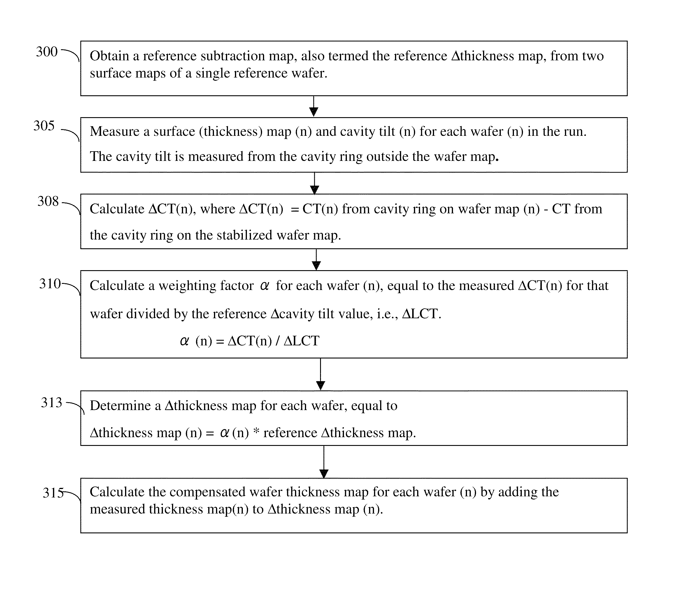
[0020]The inventive method and system is directed to monitoring and compensating for measurement error in an interferometric system caused by thermally induced changes in air index of refraction and resulting optical path length differences.

[0021]Described hereinafter is an example of a systematic method for detecting and reducing measurement errors induced into the dual channel reflection-type interferometer wafer measurement system by temperature gradients. Note that the details of the method are exemplary and not limiting. Other methods may be used to compensate for the thermally induced changes in optical path length differences, without departing from the inventive concept.

[0022]Neither the wafer temperature, the temperature gradient of the air, or the refractive index gradient of the air are easily measured. The inventive method embodiment disclosed herein provides an indirect detection of air temperature gradient, and provides a method to compensate for the measurement error ...


PUM


Abstract

Disclosed herein is a method and apparatus for reducing measurement error resulting from temperature variations across a wafer, without measuring the wafer temperature, the temperature gradient in the surrounding air, or the distribution of the index of refraction of the air.

Description

FIELD OF THE INVENTION[0001]This invention relates to measurement systems, and in particular to compensating for wafer measurement variations due to temperature variations across the wafer, particularly relating to optical interferometer measurements.BACKGROUND[0002]Dual channel reflection-type interferometers are a preferred tool used for measuring wafer shape for semiconductor processing applications. An example of such a dual channel reflection-type interferometer tool is WaferSight from KLA-Tencor. A side view diagram of a WaferSight tool 100 is shown in FIG. 1a. Wafer 102 is positioned within cavity 105. FIG. 1b shows a front view of cavity 105, showing wafer region 107 and cavity ring region 108, an annular region within the cavity but outside wafer region 107.[0003]WaferSight uses two channels. Each measures the optical interference signal from two beams, a first reflected beam from wafer surface 110, 111 and a second reflected beam reflected from internal reference surface 1...

Claims


Application Information

Patent Timeline
IPC IPC(8): G01B9/02
CPCG01B9/02007G01B21/045G01B5/0014G01B2210/44G01B2210/48
Inventor SEONG, KIBYUNGTANG, SHOUHONG
Owner KLA TENCOR TECH CORP
Why Eureka
Try Eureka