Stackable semiconductor assembly with bump/flange heat spreader and dual build-up circuitry

a technology of heat spreader and semiconductor assembly, which is applied in the association of printed circuit non-printed electric components, basic electric elements, solid-state devices, etc., can solve the problems of reducing chip feature sizes, many performance-related deficiencies remain, and multiple devices stacked in a limited space often encounter undesirable inter-device noise, so as to improve thermal and electrical performance and environmental reliability, avoid likely shifting and cracking of embedded chips during lamination, and improve manufacturing yield

Inactive Publication Date: 2015-02-10
BRIDGE SEMICON
View PDF33 Cites 7 Cited by
  • Summary
  • Abstract
  • Description
  • Claims
  • Application Information

AI Technical Summary

Benefits of technology

[0035]The present invention has numerous advantages. The bump and the flange can be integral with one another, thereby providing excellent heat spreading, electromagnetic shielding and a moisture barrier for the semiconductor device for better thermal and electrical performance as well as environmental reliability. The mechanically-formed cavity in the bump can provide a well-defined space for semiconductor device placement. As a result, the likely shifting and cracking of the embedded chip during lamination can be avoided, thereby enhancing manufacturing yield and reducing cost. The adhesive can be sandwiched between the bump and the conductive layer, between the bump and the substrate and between the flange and the substrate, thereby providing a robust mechanical bond between the heat spreader and the substrate. The first build-up circuitry can provide electrical connections to the semiconductor device with plated metal without wire bonds or solder joints, thereby increasing reliability. The first and second build-up circuitries can provide signal routing with simple circuitry patterns or flexible multi-layer signal routing with complex circuitry patterns. The plated through-hole can provide vertical signal routing between the two build-up circuitries with respective interconnect pads at both sides of the assembly, thereby providing the assembly with stacking capability.

Problems solved by technology

Furthermore, as there are significant obstacles to further reduce chip feature sizes below the nanometer range due to significant expense for material, equipment and process developments, attention has therefore shifted to packaging technologies to timely fulfill the relentless demands for a smarter and smaller device.
Despite numerous three-dimensional packaging architectures reported in the literature, many performance-related deficiencies remain.
For instance, multiple devices stacked in a limited space often encounter undesirable inter-device noise such as electromagnetic interference (EMI).
The signal integrity of the stacked devices can be adversely affected when they perform high frequency transmitting or receiving of signals.
Furthermore, as semiconductor devices are susceptible to performance degradation and immediate failure at high operating temperatures, collective heat generated from the chips enclosed in a thermally insulating material such as dielectrics can cause catastrophic damage to the assembly.
However, as most plastic material has low thermal conductivity, this plastic assembly suffers poor thermal performance and offers no electromagnetic shielding protection for the embedded chips.
ns. None of these approaches offers a proper thermal dissipation solution or effective electromagnetic protection for the embedded ch
Since the cavity in the substrate is formed by laser or plasma etching of the substrate, the major drawbacks include low throughput and high cost in forming the cavity in addition to the limited heat dissipation capability of the bottom metal layer in the structure.
Inconsistent cavity depth control of the recess in the metal plate can result in low throughput and low yield in volume production.
Furthermore, as the thick metal plate would electrically block the vertical connection to the bottom surface, resin filled holes need to be created before metallized plated through-holes can be built in the metal block.
The cumbersome process makes the manufacturing yield excessive low and costly.
Like many other cavity type approaches, this assembly suffers poor manufacturing throughput and low yield due to inconsistent cavity formation in the resin.
Furthermore, since the metal is deposited in the cavity by electroplating, it has limited thickness and does little to improve the package's thermal performance.

Method used


Image

  • Stackable semiconductor assembly with bump/flange heat spreader and dual build-up circuitry
  • Stackable semiconductor assembly with bump/flange heat spreader and dual build-up circuitry
  • Stackable semiconductor assembly with bump/flange heat spreader and dual build-up circuitry

Examples


embodiment 1

[Embodiment 1]

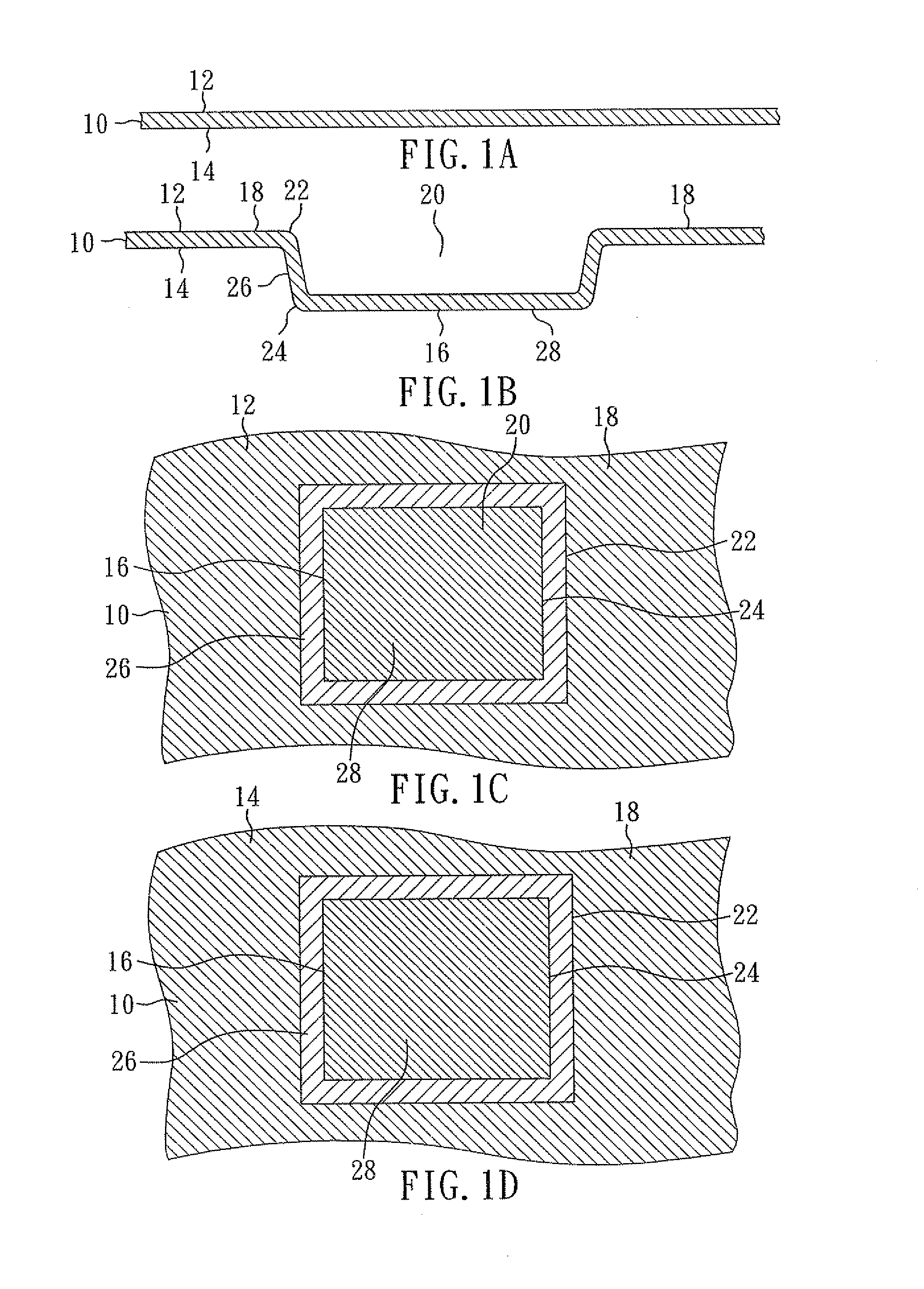
[0050]FIGS. 1A and 1B are cross-sectional views showing a method of making a bump and a flange in accordance with an embodiment of the present invention, and FIGS. 1C and 1D are top and bottom views, respectively, corresponding to FIG. 1B.

[0051]FIG. 1A is a cross-sectional view of metal plate 10 which includes opposing major surfaces 12 and 14. Metal plate 10 is illustrated as a copper plate with a thickness of 100 microns. Copper has high thermal conductivity, good flexibility and low cost. Metal plate 10 can be various metals such as copper, aluminum, alloy 42, iron, nickel, silver, gold, combinations thereof, and alloys thereof.

[0052]FIGS. 1B, 1C and 1D are cross-sectional, top and bottom views, respectively, of metal plate 10 with bump 16, flange 18 and cavity 20. Bump 16 and cavity 20 are formed by mechanically stamping metal plate 10. Thus, bump 16 is a stamped portion of metal plate 10 and flange 18 is an unstamped portion of metal plate 10.

[0053]Bump 16 is adja...

embodiment 2

[Embodiment 2]

[0115]FIGS. 8A-8H are cross-sectional views showing a method of making a stackable semiconductor assembly with a plated through-hole connected to inner pads of the thermal board according to another aspect of the present invention.

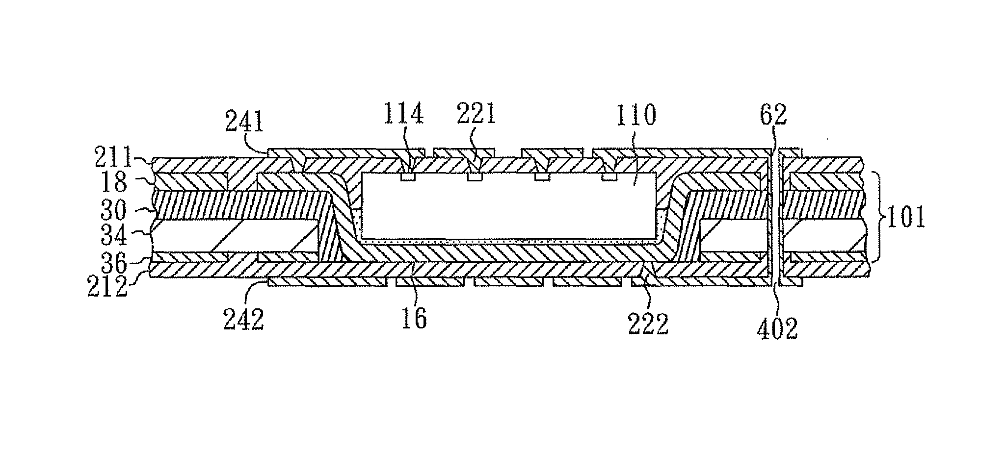
[0116]FIG. 8A is a cross-sectional view of thermal board 101, which is manufactured by the steps shown in FIGS. 1A-4E.

[0117]FIG. 8B is a cross-sectional view of the structure with through-holes 401. Through-holes 401 extend through flange 18, adhesive 30, substrate 34 and conductive layer 36 in the vertical direction. Through-holes 401 are formed by mechanical drilling and can be formed by other techniques such as laser drilling and plasma etching.

[0118]FIG. 8C is a cross-sectional view of the structure with first plated layer 60 outside through-hole 401 and connecting layer 62 and insulative filler 63 in through-hole 401. First plated layer 60 covers and extends from bump 16 and flange 18 in the upward direction. First plated layer 60 also c...

embodiments 3-4

[Embodiments 3-4]

[0134]FIGS. 9-10 are cross-sectional views showing stackable semiconductor assemblies wherein the thermal board is devoid of a substrate.

[0135]In these embodiments, a thick conductive layer 36 is applied and the substrate is omitted. For instance, conductive layer 36 has a thickness of 130 microns (rather than 30 microns) so that it can be handled without warping or wobbling. If a base is created, as shown in FIG. 10, base 64 and second inner pad 183 are therefore thicker, and thermal board 102 is devoid of a substrate. Accordingly, base 64 has a first thickness where it is adjacent to the bump 16 and a second thickness where it is adjacent to the adhesive 30 that is larger than the first thickness, and base 64 and second inner pad 183 have the same thickness where closest to one another and different thickness where base 64 is adjacent to bump 16 and are coplanar with one another at a surface that faces in the downward direction.

[0136]As mentioned above, adhesive 3...


PUM


Abstract

A stackable semiconductor assembly includes a semiconductor device, a heat spreader, an adhesive, a plated through-hole, first build-up circuitry and second build-up circuitry. The heat spreader includes a bump and a flange. The bump defines a cavity. The semiconductor device is mounted on the bump at the cavity, electrically connected to the first build-up circuitry and thermally connected to the bump. The bump extends into an opening in the adhesive and the flange extends laterally from the bump at the cavity entrance. The first build-up circuitry and the second build-up circuitry extend beyond the semiconductor device in opposite vertical directions. The plated through-hole extends through the adhesive and provides signal routing between the first build-up circuitry and the second build-up circuitry. The heat spreader provides heat dissipation for the semiconductor device.

Description

CROSS REFERENCE TO RELATED APPLICATION[0001]This application claims the benefit of filing date of U.S. Provisional Application Ser. No. 61 / 415,862, entitled “SEMICONDUCTOR CHIP ASSEMBLY WITH BUMP / BASE HEAT SPREADER, CAVITY IN BUMP AND EXTENDED CONDUCTIVE TRACE” filed Nov. 22, 2010 under 35 USC §119(e)(1).BACKGROUND OF THE INVENTION[0002]1. Field of the Invention[0003]The present invention relates to a semiconductor assembly, and more particularly to a stackable semiconductor assembly that includes a semiconductor device, a heat spreader, an adhesive, a plated through-hole and dual build-up circuitry.[0004]2. Description of Related Art[0005]In the field of electronic systems, there is a continuous need to improve performance and reduce size and weight. Many approaches have been proposed to meet these requirements and strike a balance between performance optimization, time-to-market expedition and cost reduction through the use of different architectures, materials, equipment, process...

Claims


Application Information

Patent Timeline
Patent Type & Authority Patents(United States)
IPC IPC(8): H01L23/34H01L21/56H01L23/00H01L23/31H01L23/367H01L23/498H01L23/538H01L23/552H01L25/10H05K1/02H05K1/18
CPCH01L23/3121H01L21/56H01L23/3677H01L23/49827H01L23/5389H01L23/552H01L24/19H01L24/20H01L24/24H01L24/82H01L25/105H05K1/0207H01L2224/04105H01L2224/1132H01L2224/1146H01L2224/11849H01L2224/12105H01L2224/19H01L2224/2101H01L2224/211H01L2224/215H01L2224/221H01L2224/24101H01L2224/24221H01L2224/2929H01L2224/29339H01L2224/82106H01L2224/83192H01L2224/83862H01L2225/1035H01L2225/1041H01L2225/1058H01L2924/01012H01L2924/01013H01L2924/01029H01L2924/01079H01L2924/01082H01L2924/09701H01L2224/131H01L2924/01005H01L2924/01006H01L2924/01023H01L2924/01033H01L2924/0104H01L2924/01047H01L2924/01074H01L2924/01075H01L2924/01087H01L2924/014H01L2224/16225H01L2225/1023H01L2224/73267H01L2924/3511H01L2224/06181H05K1/186H01L2924/0001H01L2224/92244H01L2224/13099H01L2924/1461H01L2224/0401H01L2924/181H01L2924/14H01L2924/15153H01L2924/00
Inventor LIN, CHARLES W. C.WANG, CHIA-CHUNG
Owner BRIDGE SEMICON
Why Eureka
Try Eureka