3D semiconductor interposer for heterogeneous integration of standard memory and split-architecture processor

a semiconductor interposer and split-architecture technology, applied in semiconductor devices, semiconductor/solid-state device details, electrical devices, etc., can solve the problems of over-long signal paths of the standard interposer connecting the wide i/o memory to the second chip, supply problems, thermal dissipation issues for the sub-chips, etc., to avoid unbalanced thermo-mechanical stress within the device, minimize the needed board real estate, and enhance device reliability

Active Publication Date: 2015-02-17
TEXAS INSTR INC
View PDF2 Cites 21 Cited by
  • Summary
  • Abstract
  • Description
  • Claims
  • Application Information

AI Technical Summary

Benefits of technology

[0010]It is a technical advantage that applicants' solution provides an approximately symmetrical construction of the stacked-chip device, thus minimizing the needed board real estate and avoiding unbalanced thermo-mechanical stress within the device, enhancing device reliability.
[0011]It is another technical advantage of applicants' solution that the two chips of the split SOC architecture, which require involved front-end process flows at the cutting edge of technology and are thus valuable, do not need TSVs so that the required TSVs remain restricted to the two silicon interposers, keeping costs as low as possible.
[0012]As another technical advantage, the use of TSVs provides significantly lower inductance and resistance than wire bonds and also good inductance scaling with shorter and smaller future TSVs.

Problems solved by technology

Applicants found that the vertical assembly, in any order, causes supply problems (IR drop limitation) and thermal dissipation issues for the sub-chips.
The signal paths of the standard interposer for connecting the wide I / O memory to the second chip would become excessively long.
Furthermore, the assembly would be non-symmetrical and result in an overhang of the memory chip to one side, causing a size increase of the overall device, leading to non-balanced stresses and reliability issues.

Method used


Image

  • 3D semiconductor interposer for heterogeneous integration of standard memory and split-architecture processor
  • 3D semiconductor interposer for heterogeneous integration of standard memory and split-architecture processor
  • 3D semiconductor interposer for heterogeneous integration of standard memory and split-architecture processor

Examples


Embodiment Construction

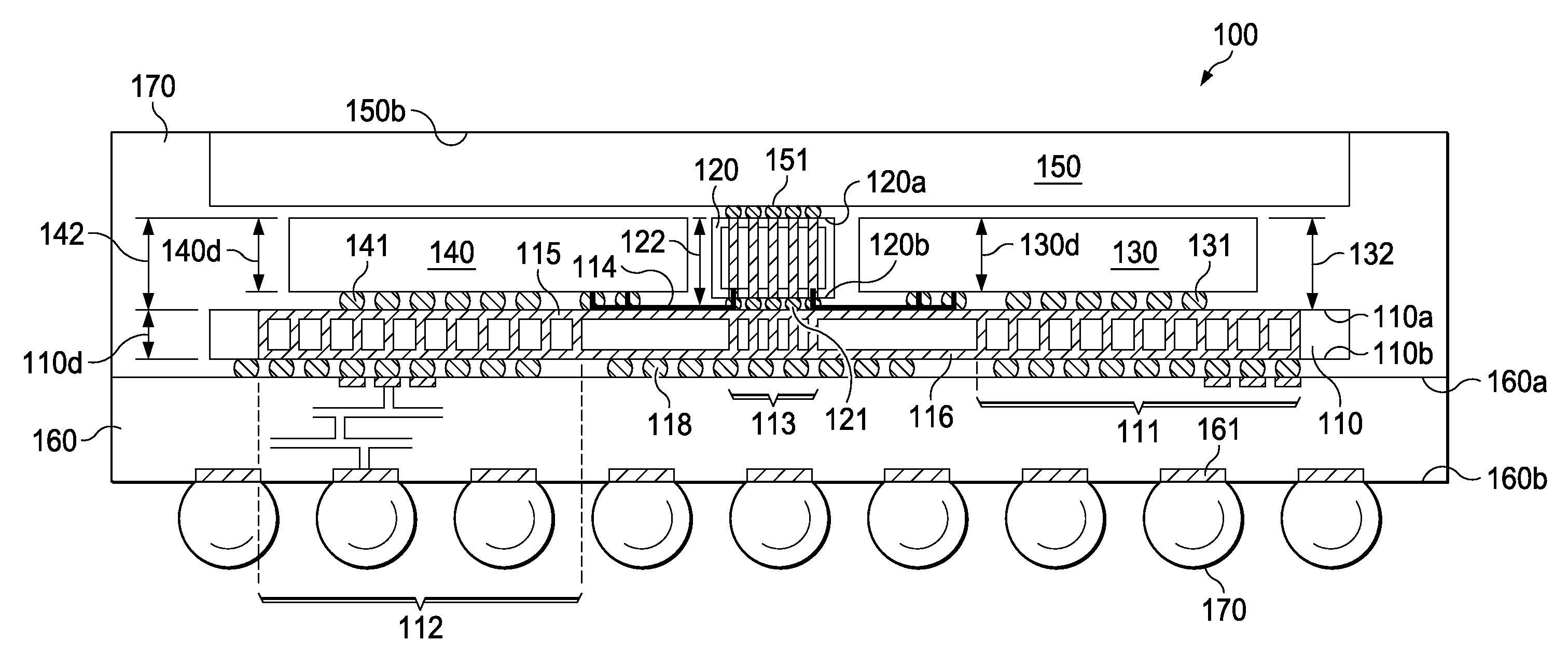
[0016]FIG. 1 illustrates an exemplary semiconductor device generally designated 100 as an embodiment of the invention. Device 100 includes a first silicon interposer 110, a second silicon interposer 120, a first semiconductor chip 130, a second semiconductor chip 140, and a third semiconductor chip 150. Device 100 further includes a substrate 160, and may also include a packaging compound 170 encapsulating the interposers 110 and 120, first chip 130 and second chip 140, and at least portions of third chip 150. The not-encapsulated surface 150b of third chip 150 may serve as an attachment site for a heat spreader or heat sink, promoting effective cooling of stacked device 100.

[0017]As FIG. 1 shows, first silicon interposer 110 has a thickness 110d, a first surface 110a and an opposite second surface 110b; thickness 110d is preferably 50 μm, but other interposers may be thicker of thinner. A plurality of through-silicon vias (TSVs) extend through first interposer 110 from the first su...


PUM


Abstract

A standard memory chip (150) is vertically assembled with two processor chips (130, 140) of split architecture by means of a small silicon interposer (120) stacked onto a large silicon interposer (110); both interposers include through-silicon vias (TSVs), while the chips are free of TSVs. The TSVs of small interposer (120) connect to the memory chip (150) and to the bottom interposer (110). Symmetrically positioned relative to interposer (120), and connected to it by short signal traces, chips (130, 140) are attached to the TSVs of interposer 110, which in turn is attached to a substrate (160) with supply connections.

Description

FIELD OF THE INVENTION[0001]The present invention is related in general to the field of semiconductor devices and processes, and more specifically to the use of two semiconductor interposers for vertically stacking chips with split architecture.DESCRIPTION OF RELATED ART[0002]Since the invention of the integrated circuit, the course of circuit development was in the direction of combining ever more electronic functions into the circuit layout on a single chip. A well known example is the combination of logic and memory functions on a single chip. The functions are constructed from electrical components such as resistors, capacitors, diodes, and transistors, which in turn are realized by layouts on the chip. Comparing the layouts of contemporary chips it becomes evident that the fabrication of the components for some layouts needs a higher number of process steps than the fabrication of the components for other layouts.[0003]The discrepancy in the number of fabrication steps is aggra...

Claims


Application Information

Patent Timeline
Patent Type & Authority Patents(United States)
IPC IPC(8): H01L23/48H01L23/52H01L25/065
CPCH01L25/065H01L2224/16225H01L2225/0652H01L25/0652H01L25/18H01L2225/06517H01L2225/06548H01L23/147H01L23/49816H01L23/5384H01L23/5385H01L2924/01322H01L2224/1308H01L2224/81825H01L24/13H01L24/16H01L2224/131H01L2224/13147H01L2224/16227H01L2224/16238H01L2224/73253H01L2224/81447H01L2224/81455H01L2224/81464H01L2224/8181H01L2224/81815H01L2924/15192H01L2924/15311H01L2924/157H01L2924/18161H01L2224/16503H01L24/81H01L25/50H01L2224/16235H01L2924/1434H01L2924/00H01L2924/014H01L2924/00014H01L21/56H01L23/49827H01L2224/81801
Inventor LYNE, KEVINWACHTLER, KURT P.
Owner TEXAS INSTR INC
Why Eureka
Try Eureka