Hybrid-integrated photonic chip package

a chip and integrated technology, applied in the field of hybrid integrated chip packages, can solve the problems of high bandwidth, low power, reliability and low cost, and the inability of existing interconnection technologies to provide suitable communication characteristics, and achieve the bandwidth, size, power requirements of input/output (i/o) interfaces, and the difficulty of scaling these photonic components to meet the bandwidth, power requirements, and reliability of future chips

Active Publication Date: 2015-03-03
ORACLE INT CORP
View PDF5 Cites 50 Cited by
  • Summary
  • Abstract
  • Description
  • Claims
  • Application Information

AI Technical Summary

Benefits of technology

[0010]One embodiment of the present disclosure provides a chip package that includes: an integrated circuit having a front surface with integrated-circuit connector pads; integrated-circuit electrical connectors electrically coupled to the integrated-circuit connector pads; a substrate having a top surface, facing the front surface, with first substrate connector pads electrically coupled to the integrated-circuit electrical connectors, and second substrate connector pads; and optical-integrated-circuit electrical connectors electrically coupled to the second substrate connector pads. Moreover, the chip package includes an optical integrated circuit having a front surface, facing the top surface, with optical-integrated-circuit connector

Problems solved by technology

As integrated-circuit (IC) technology continues to scale to smaller critical dimensions, it is increasingly difficult for existing interconnection technologies to provide suitable communication characteristics, such as: high bandwidth, low power, reliability and low cost.
However, while photonic technologies based on vertical cavity surface-emitting lasers (VCSELs) and optical fibers are typically a convenient and cost-effective soluti

Method used


Image

  • Hybrid-integrated photonic chip package
  • Hybrid-integrated photonic chip package
  • Hybrid-integrated photonic chip package

Examples


Embodiment Construction

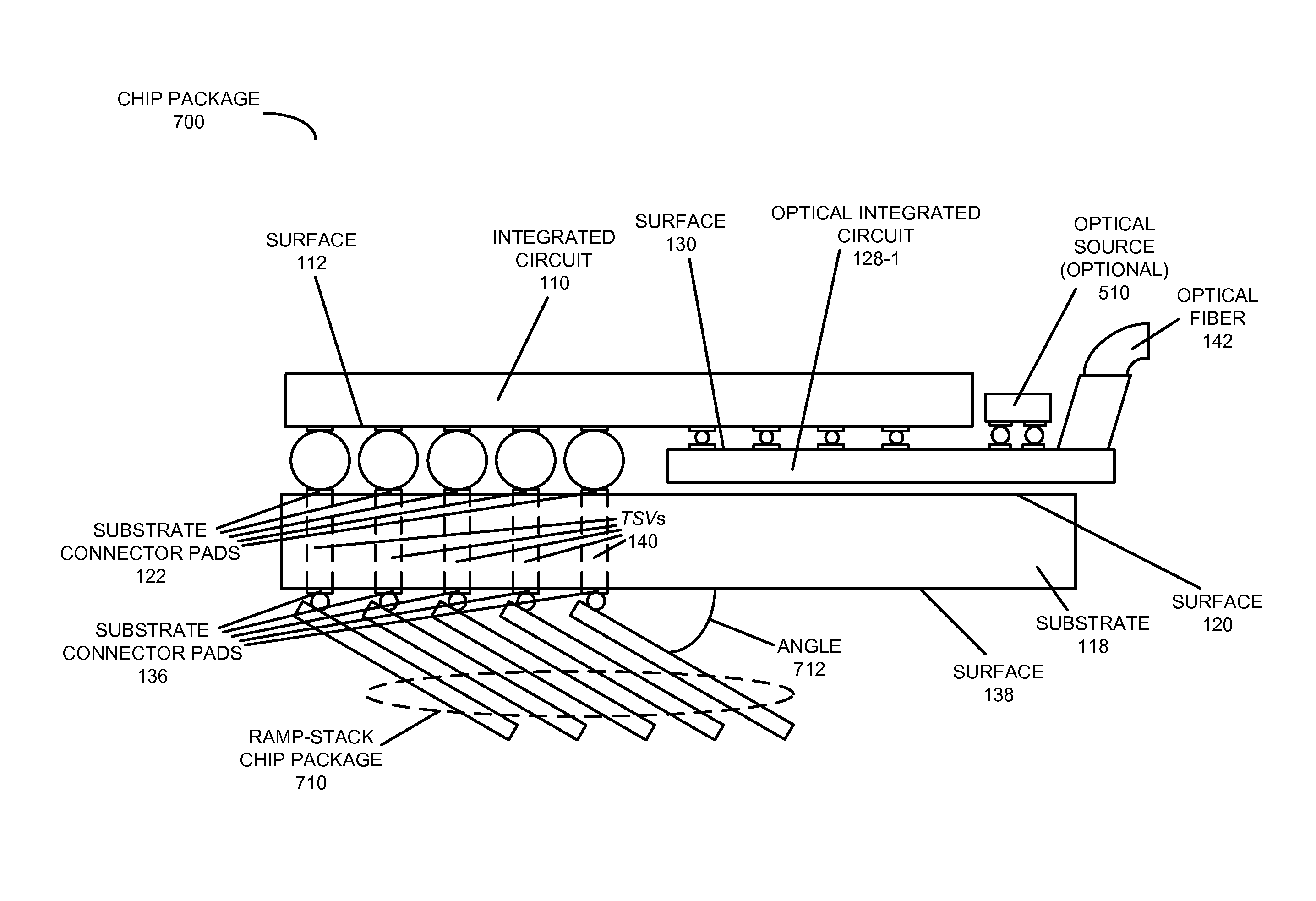
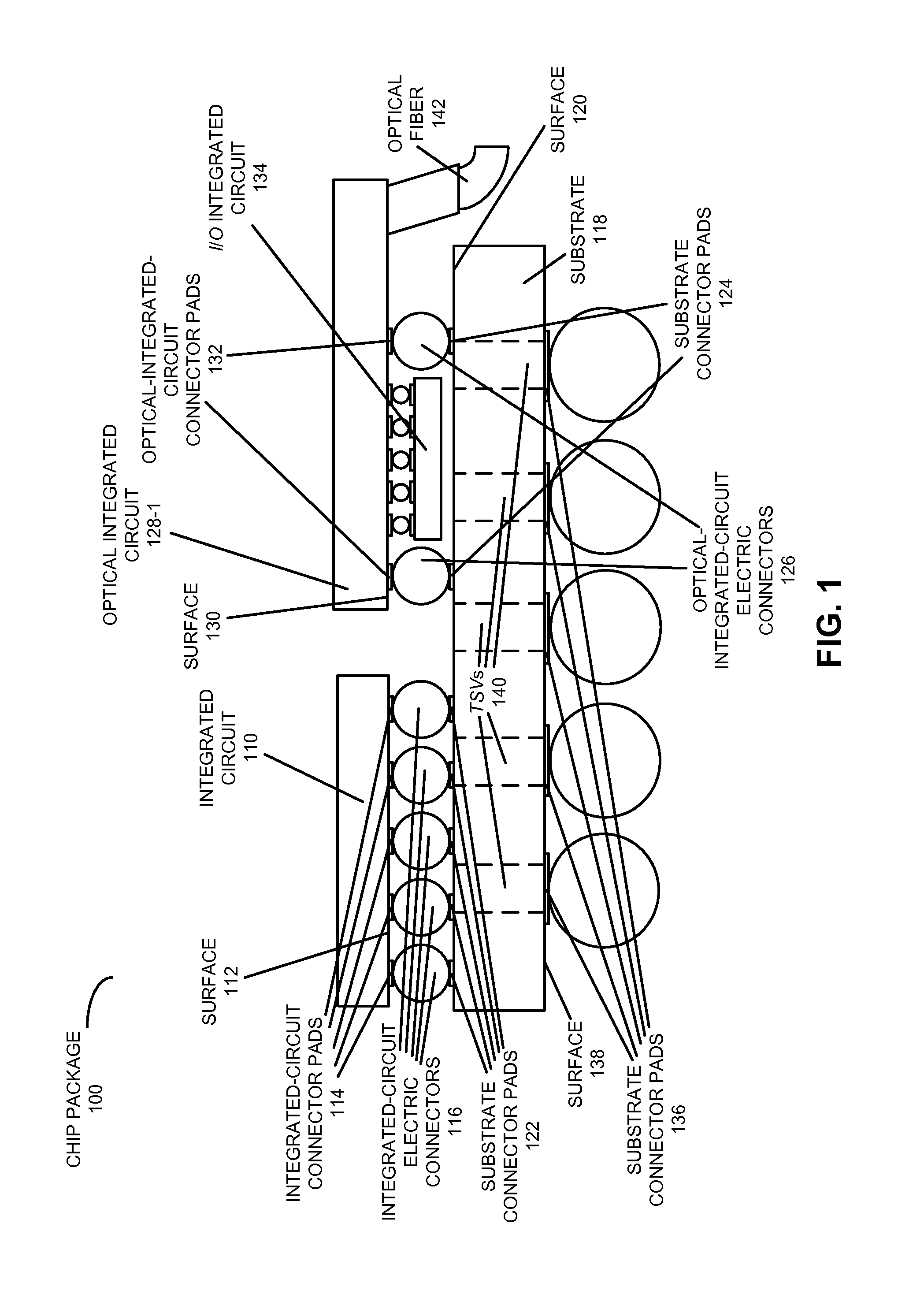
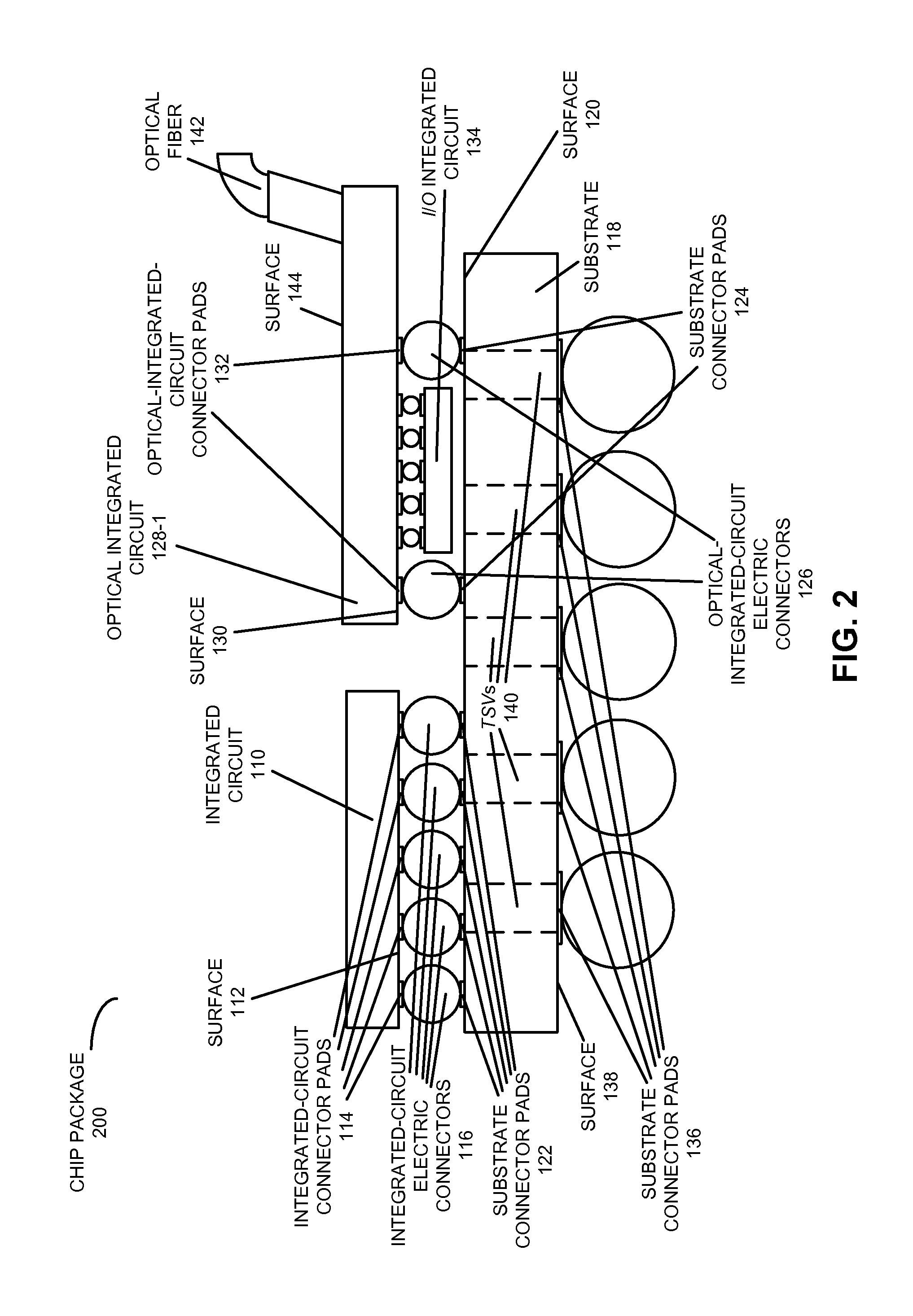
[0035]Embodiments of a chip package, a system that includes the chip package, and a technique for communicating electrical signals between an integrated circuit and an optical integrated circuit in the chip package are described. This chip package includes an optical integrated circuit (such as a hybrid integrated circuit) and an integrated circuit, which are adjacent to each other on the same side of a substrate in the chip package. The integrated circuit includes electrical circuits, such as memory or a processor, and the optical integrated circuit communicates optical signals with very high bandwidth. In addition, an input / output (I / O) integrated circuit is coupled to the optical integrated circuit between the substrate and the optical integrated circuit. This I / O integrated circuit serializes and deserializes data in the electrical signals communicated between the integrated circuit and the optical integrated circuit.

[0036]By integrating the optical integrated circuit, the integ...


PUM


Abstract

A chip package includes an optical integrated circuit (such as a hybrid integrated circuit) and an integrated circuit that are adjacent to each other on the same side of a substrate in the chip package. The integrated circuit includes electrical circuits, such as memory or a processor, and the optical integrated circuit communicates optical signals with very high bandwidth. In addition, an input/output (I/O) integrated circuit is coupled to the optical integrated circuit between the substrate and the optical integrated circuit. This I/O integrated circuit includes high-speed I/O circuits and energy-efficient driver and receiver circuits and communicates with optical devices on the optical integrated circuit. By integrating the optical integrated circuit, the integrated circuit and the I/O integrated circuit in close proximity, the chip package may facilitate improved performance compared to chip packages with electrical interconnects.

Description

GOVERNMENT LICENSE RIGHTS[0001]This invention was made with United States government support under Agreement No. HR0011-08-9-0001 awarded by DARPA. The United States government has certain rights in the invention.CROSS-REFERENCE TO RELATED APPLICATIONS[0002]This application is related to U.S. Non-provisional patent application Ser. No. 14 / 047,910, entitled “Hybrid-Integrated Photonic Chip Package with an Interposer,” by Hiren D. Thacker, Frankie Y. Liu, Robert D. Hopkins, Jon Lexau, Xuezhe Zheng, Guoliang Li, Ivan Shubin, Ronald Ho, John E. Cunningham, and Ashok V. Krishnamoorthy, filed on 7 Oct. 2013; and to U.S. Non-provisional patent application Ser. No. 14 / 047,978, entitled “Hybrid-Integrated Photonic Chip Package with an Interposer,” by Hiren D. Thacker, Ashok V. Krishnamoorthy, Robert D. Hopkins, Jon Lexau, Xuezhe Zheng, Ronald Ho, Ivan Shubin, and John E. Cunningham, filed on 7 Oct. 2013, the contents of both of which are herein incorporated by reference.BACKGROUND[0003]1. Fi...

Claims


Application Information

Patent Timeline
IPC IPC(8): G02B6/12
CPCG02B6/12G02B6/428G02B6/42H05K1/141H05K2201/046H05K2201/10121H01L2225/06534H01L24/16H01L24/17H01L25/0652H01L2224/0401H01L2224/16145H01L2224/16225H01L2224/16235H01L2224/1703H01L2225/06517H01L2924/15311H01L2924/157H01L2924/15787H01L2924/15788H01L2225/06513H01L2225/06565H01L2225/06548G02B6/4274
Inventor THACKER, HIREN D.KRISHNAMOORTHY, ASHOK V.HOPKINS, II, ROBERT DAVIDLEXAU, JONHO, RONALDCUNNINGHAM, JOHN E.
Owner ORACLE INT CORP
Why Eureka
Try Eureka