Semiconductor photocatalyst coated with graphitic carbon film and method of fabricating the same

a technology of graphitic carbon film and photocatalyst, which is applied in the direction of physical/chemical process catalysts, metal/metal-oxide/metal-hydroxide catalysts, non-metal conductors, etc., can solve the problems of agglomeration phenomenon, low photoconversion efficiency, and difficulty in industrial use of substances, etc., to achieve the effect of increasing the photoconversion efficiency of photocatalys

Inactive Publication Date: 2015-03-24
KOREA ADVANCED INST OF SCI & TECH
View PDF4 Cites 1 Cited by
  • Summary
  • Abstract
  • Description
  • Claims
  • Application Information

AI Technical Summary

Benefits of technology

[0019]According to the semiconductor photocatalyst coated with a graphitic carbon film of the present invention, a graphitic carbon film having a thickness of 1 nm or less is uniformly bound to the surface of a semiconductor substance. Therefore, the photoelectrons generated from the semiconductor catalyst can often flow to the outside thereof through a bound conductive carbon film without recombining with the holes in the substance, thereby increasing the photoconversion efficiency of the photocatalyst.

Problems solved by technology

The existing semiconductor photocatalysts, however, have a problem in that the photoconversion efficiency is low because electron-hole recombination is frequently generated by various defects in semiconductor substances.
However, the conditions for forming a semiconductor substance with a high-purity single crystal are very strict and the forming process is complicated, so that it is difficult to use the substance for industrial purposes.
In addition, a substance formed with a dimension of several nanometers, which is smaller than the electron diffusion length, has high surface energy, and thereby often exhibit an agglomeration phenomenon, thus this is not considered as an effective solution.
The substances have a problem, however, in that they cannot be applied to semiconductor substances having a complicated structure because the manufacturing method and the forming conditions are restrictive.

Method used


Image

  • Semiconductor photocatalyst coated with graphitic carbon film and method of fabricating the same
  • Semiconductor photocatalyst coated with graphitic carbon film and method of fabricating the same
  • Semiconductor photocatalyst coated with graphitic carbon film and method of fabricating the same

Examples


Embodiment Construction

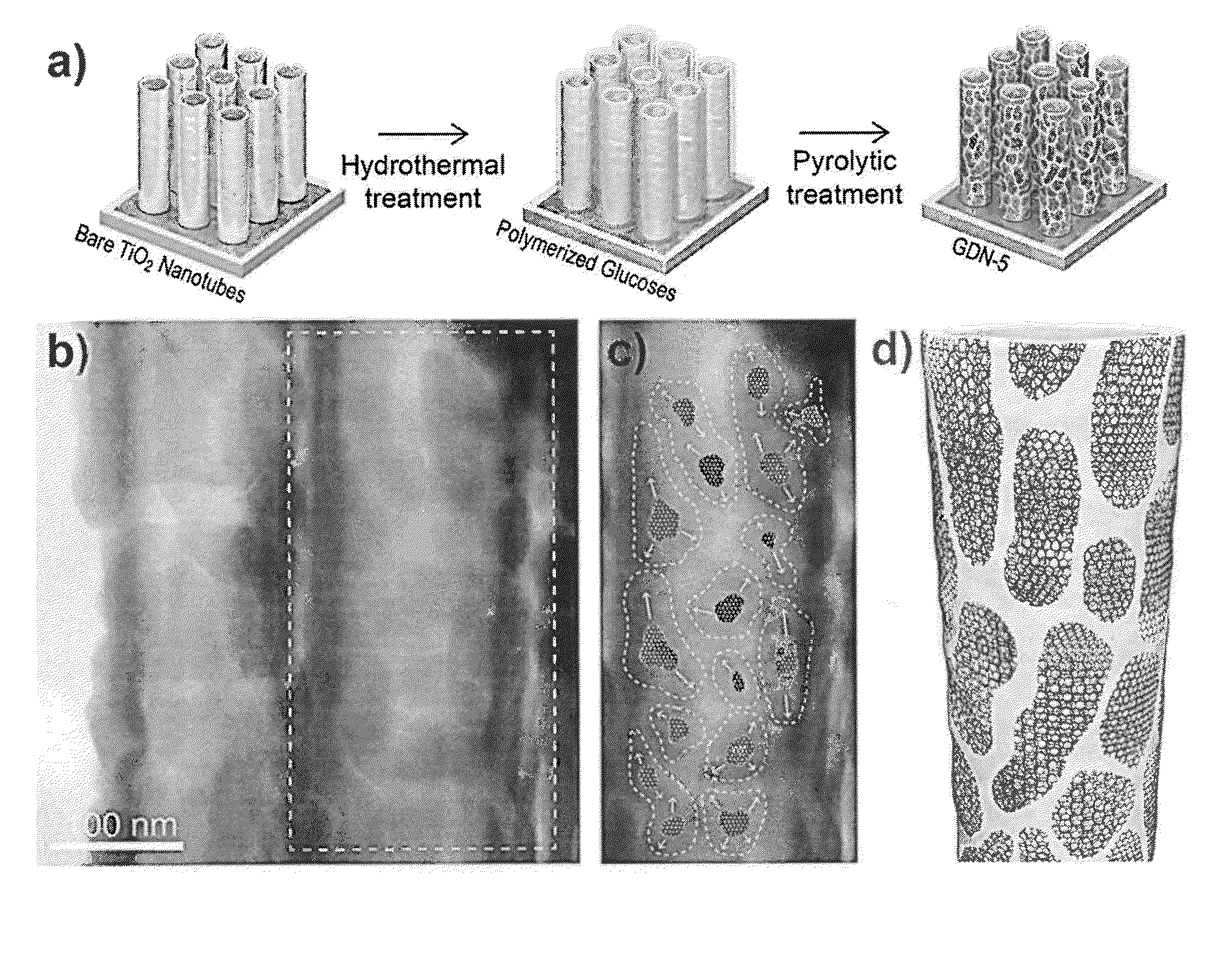
[0025]An embodiment of the present invention provides a method of fabricating a semiconductor coated with a carbon film which includes a first step of preparing a semiconductor to be coated with a carbon film, a second step of introducing the semiconductor into an aqueous solution and heat treating to form a. gel type glucose onto the surface of the semiconductor, and a third step of heat treating the resultant of the second step to form the semiconductor coated with the carbon film.

[0026]FIG. 1 is a schematic diagram showing the synthesizing and growing process of a semiconductor photocatalyst coated with a graphitic carbon film. First, it is necessary to prepare a semiconductor to be coated with a carbon film, but the present invention is not limited thereto. In the present embodiment, the nanotube arrangement of the titanium dioxide (TiO2) that is a semiconductor photocatalyst is grown on a titanium substrate by an electro-metallurgical process. The detailed fabricating method of...


PUM

PropertyMeasurementUnit
thicknessaaaaaaaaaa
thicknessaaaaaaaaaa
Time-aaaaaaaaaa

Abstract

A semiconductor of which a substance such as a semiconductor photocatalyst is uniformly coated on the surface thereof with a graphitic carbon film and a method of fabricating the same are disclosed. According to the inventive method, a graphitic carbon film having a thickness of 1 nm or less is uniformly formed on the surface of the semiconductor by performing hydrothermal synthesis and pyrolysis on glucose, so as to keep the original structure crystallinity of the semiconductor photocatalyst to be a support of the carbon film.

Description

CROSS REFERENCE TO RELATED APPLICATIONS[0001]This application claims priority to Korean Patent Application No. 10-2012-0078747, filed on Jul. 19, 2012 in the Korean Intellectual Property Office, the entire disclosure of which is incorporated herein by reference.BACKGROUND OF THE INVENTION[0002]1. Field of the Invention[0003]The present invention relates to a method of fabricating a graphitic carbon film on the surface of a semiconductor and a semiconductor photocatalyst fabricated by the same. In more detail, the present invention relates to a semiconductor of which a substance such as a semiconductor photocatalyst, which has important electrochemical properties, is coated on the surface thereof with a graphitic carbon film having a thickness of 1 nm or less, so as to ensure attenuated electron-hole recombination while keeping the original structure and properties of the semiconductor substance, and a method of fabricating the same.[0004]2. Background Art[0005]Toxic substances (carb...

Claims


Application Information

Patent Timeline
Patent Type & Authority Patents(United States)
IPC IPC(8): B01J21/18H05B7/085H01B1/06H01B1/02B01J23/00H01L21/02H01L29/06H01L51/00
CPCH01L21/0228H01L29/0603H01L51/0045Y10S977/811Y10S977/823Y10S977/90H10K85/20B01J37/02C01G23/047B82B1/00B82B3/00
Inventor KANG, JEUNG-KULEE, DONG-KIHAN, KYU-SUNGSHIN, WEON-HOLEE, JUNG-WOOCHOI, JUNG-HOONCHOI, KYUNG-MINLEE, YEOB
Owner KOREA ADVANCED INST OF SCI & TECH
Why Eureka
Try Eureka