RF bus and RF return bus for plasma chamber electrode

a return bus and electrode technology, applied in the field of coupling rf power, can solve the problems of failure of capacitors reduce the inductance of the electrical connection, reduce the risk of atmospheric arcing, and reduce the inductance advantageously the peak voltage within the rf circuitry

Active Publication Date: 2015-03-31
APPLIED MATERIALS INC
View PDF54 Cites 153 Cited by
  • Summary
  • Abstract
  • Description
  • Claims
  • Application Information

AI Technical Summary

Benefits of technology

[0011]Advantageously, the parallel RF bus and RF return bus conductors reduce the inductance of the electrical connection between the RF input and the plasma chamber electrode. This reduced inductance advantageously reduces the peak voltages within the RF circuitry. This helps reduce the risk of atmospheric arcing (i.e., electrical discharge) in the portions of the RF circuitry that are exposed to atmosphere, and it helps reduce the risk of failure of the capacitors within the RF circuitry.
[0012]In another aspect of the invention, the RF bus conductor has a transverse cross section having a longest dimension oriented perpendicular to the surface of the plasma chamber electrode that is closest to the RF bus conductor. Advantageously, this orientation of the RF bus conductor reduces parasitic capacitive coupling of RF power to areas of the electrode other than locations where an electrical connection to the electrode is intended.

Problems solved by technology

Such high peak voltage is undesirable because it can cause atmospheric arcing (i.e., electrical discharge) in the portions of the RF circuitry that are exposed to atmosphere, and it can cause failure of the capacitors within the RF circuitry.

Method used


Image

  • RF bus and RF return bus for plasma chamber electrode
  • RF bus and RF return bus for plasma chamber electrode
  • RF bus and RF return bus for plasma chamber electrode

Examples


second embodiment

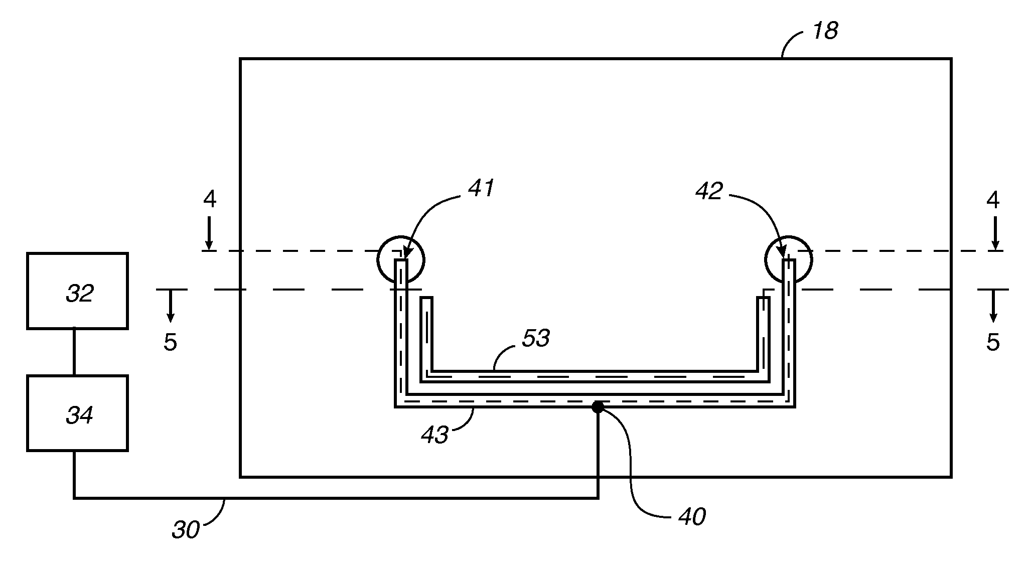
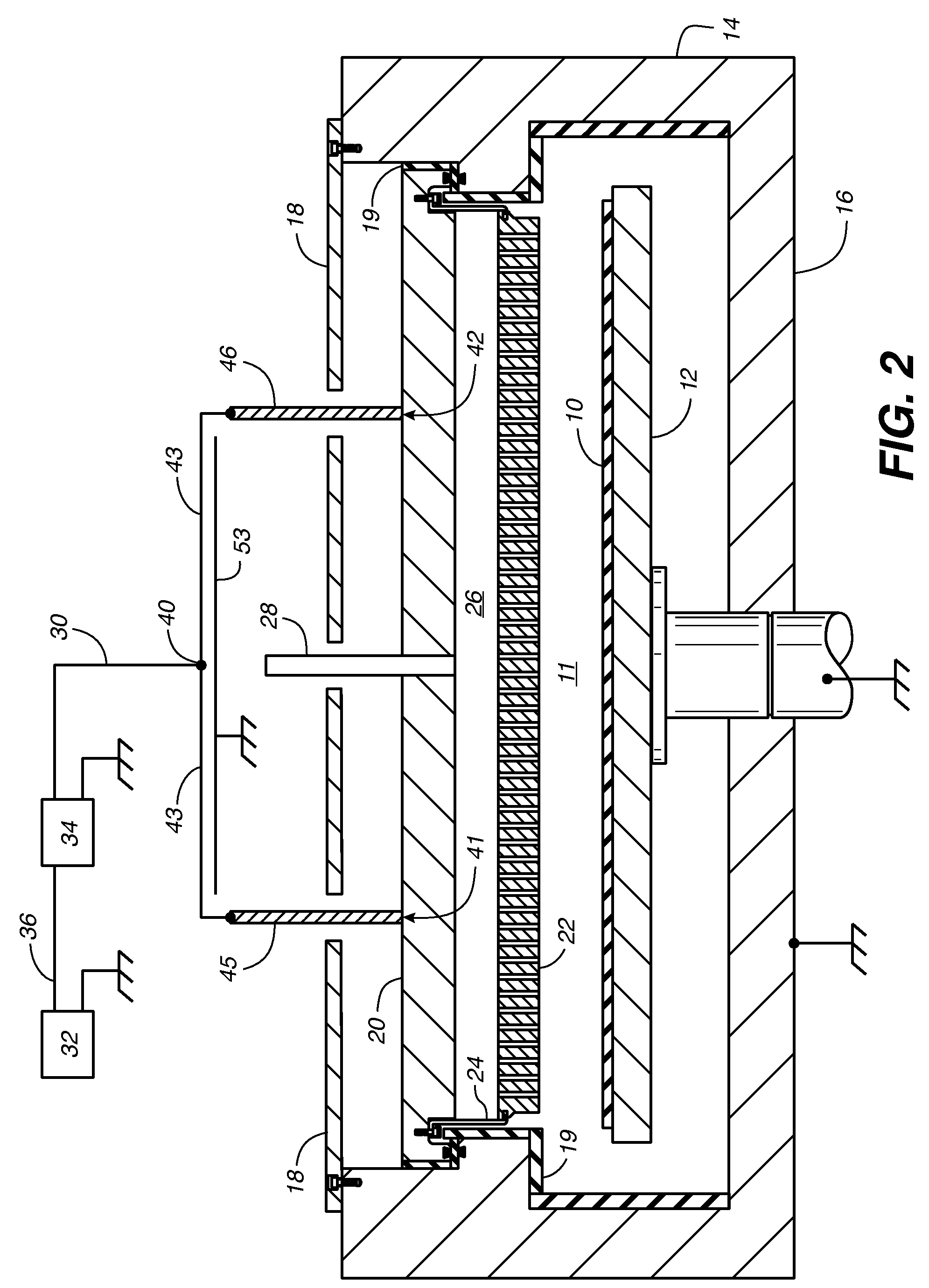
[0052]In a second embodiment, the capacitance between an RF bus conductor 43, 44 and its corresponding RF return bus conductor 53, 54 is greater than the capacitance between that RF bus conductor and the electrically grounded chamber wall 14-18.

third embodiment

[0053]In a third embodiment, an RF bus conductor 43, 44 and its corresponding RF return bus conductor 53, 54 have respective surfaces that are parallel and face each other, wherein the two surfaces are separated by a spacing that is less than the spacing between the RF bus conductor and any of the electrically grounded chamber walls that are parallel to the first surface.

fourth embodiment

[0054]In a fourth embodiment, an RF bus conductor 43, 44 and its corresponding RF return bus conductor 53, 54 have respective surfaces that are parallel and face each other, wherein the two surfaces are separated by a spacing that is less than the width of either of the two surfaces in any direction.

[0055]In any of the embodiments defined above, one can maximize the benefit of reducing the inductance of the entire RF current path from the output of the impedance matching network 34 to the plasma by maximizing the fraction of such RF current path that is implemented by the parallel, closely-spaced RF bus and RF return bus conductors of the present invention. In other words, it is beneficial for the RF bus and RF return bus conductors to occupy a substantial fraction of such RF current path.

[0056]For example, this “substantial fraction” criterion is satisfied if the RF bus conductor occupies at least one-half the length of the electrical connection path extending from the output of th...


PUM

PropertyMeasurementUnit
lengthaaaaaaaaaa
widthaaaaaaaaaa
capacitanceaaaaaaaaaa

Abstract

For coupling RF power from an RF input of a plasma chamber to the interior of a plasma chamber, an RF bus conductor is connected between the RF input and a plasma chamber electrode. In one embodiment, an RF return bus conductor is connected to an electrically grounded wall of the chamber, and the RF bus conductor and the RF return bus conductor have respective surfaces that are parallel and face each other. In another embodiment, the RF bus conductor has a transverse cross section having a longest dimension oriented perpendicular to the surface of the plasma chamber electrode that is closest to the RF bus conductor.

Description

CROSS REFERENCE TO RELATED APPLICATIONS[0001]This patent application claims priority of U.S. provisional patent application No. 61 / 152,601 filed Feb. 13, 2009 by Carl A. Sorensen et al.TECHNICAL FIELD[0002]The invention relates generally to coupling RF power to an electrode of a plasma chamber used for fabricating electronic devices such as semiconductors, displays, solar cells, and solid state light emitting devices. The invention relates more specifically to RF bus and RF return bus conductors connected to the electrode, and to the orientation of the RF bus conductor relative to the electrode. The invention improves the efficiency of coupling RF power to plasma within the chamber.BACKGROUND ART[0003]Plasma chambers commonly are used to perform processes for fabricating electronic devices such as semiconductors, displays and solar cells. Such plasma fabrication processes include chemical vapor deposition of semiconductor, conductor or dielectric layers on the surface of a workpiece...

Claims


Application Information

Patent Timeline
Patent Type & Authority Patents(United States)
IPC IPC(8): H01L21/3065C23C16/505H01J37/32
CPCH01J37/32174H01J37/32091
Inventor SORENSEN, CARL A.KUDELA, JOZEFTINER, ROBIN L.ANWAR, SUHAILWHITE, JOHN M.
Owner APPLIED MATERIALS INC
Why Eureka
Try Eureka