Circuit component and method of making the same

a technology of circuit components and components, applied in the direction of conductors, semiconductor/solid-state device details, instruments, etc., can solve the problems of insufficient contact between electrodes and substrates, inability to obtain satisfactory connection between substrates and ic chips, and inability to completely prevent warpage, so as to suppress warpage of substrates and ic chips, and reduce the amount of electrically conductive adhesive

Active Publication Date: 2015-04-28
RESONAC CORPORATION
View PDF20 Cites 2 Cited by
  • Summary
  • Abstract
  • Description
  • Claims
  • Application Information

AI Technical Summary

Benefits of technology

[0009]According to the circuit component of the one aspect of the present invention, at the time of making the circuit component, when the substrate and the IC chip are pulled toward each other and thus deformed by thermal shrinkage or cure shrinkage of the electrically conductive adhesive that fills the space between the surface of the substrate and the non-electrode surface, the electrically conductive particles in the first state that are placed so as to be in contact with both the surface of the substrate and the non-electrode surface counteract the deformation of the substrate and the IC chip, and the warpage of the substrate and the IC chip is suppressed. Consequently, the interval between the surface of the substrate and the bump electrode is suppressed from becoming larger, and the bump electrode and the substrate are satisfactorily connected to each other by the electrically conductive particles in the second state that are placed so as to dig into the bump electrode. As a result, the substrate and the IC chip can be satisfactorily connected to each other.
[0018]According to the present invention, it is possible to provide a circuit component that enables satisfactory connection between a substrate and an IC chip and a method of making the same.

Problems solved by technology

If such an IC chip and a substrate are connected to each other using an electrically conductive adhesive, the substrate and the IC chip are pulled toward each other by thermal shrinkage or cure shrinkage of the electrically conductive adhesive that fills a portion in which bump electrodes are not provided, and the substrate and the IC chip deform such that the interval therebetween becomes smaller in the portion in which the bump electrodes are not provided, so that warpage occurs wholly.
If the warpage of the substrate and the IC chip occurs, the interval between the bump electrodes and the substrate may be larger in a portion in which the interval between the substrate and the IC chip is larger, the bump electrodes and the substrate may not be in sufficient contact with each other, and satisfactory connection between the substrate and the IC chip may not be obtained.

Method used


Image

  • Circuit component and method of making the same
  • Circuit component and method of making the same
  • Circuit component and method of making the same

Examples


Embodiment Construction

[0029]Hereinafter, a circuit component and a method of making the same according to an embodiment of the present invention are described in detail with reference to the drawings.

[0030][Substrate and IC Chip]

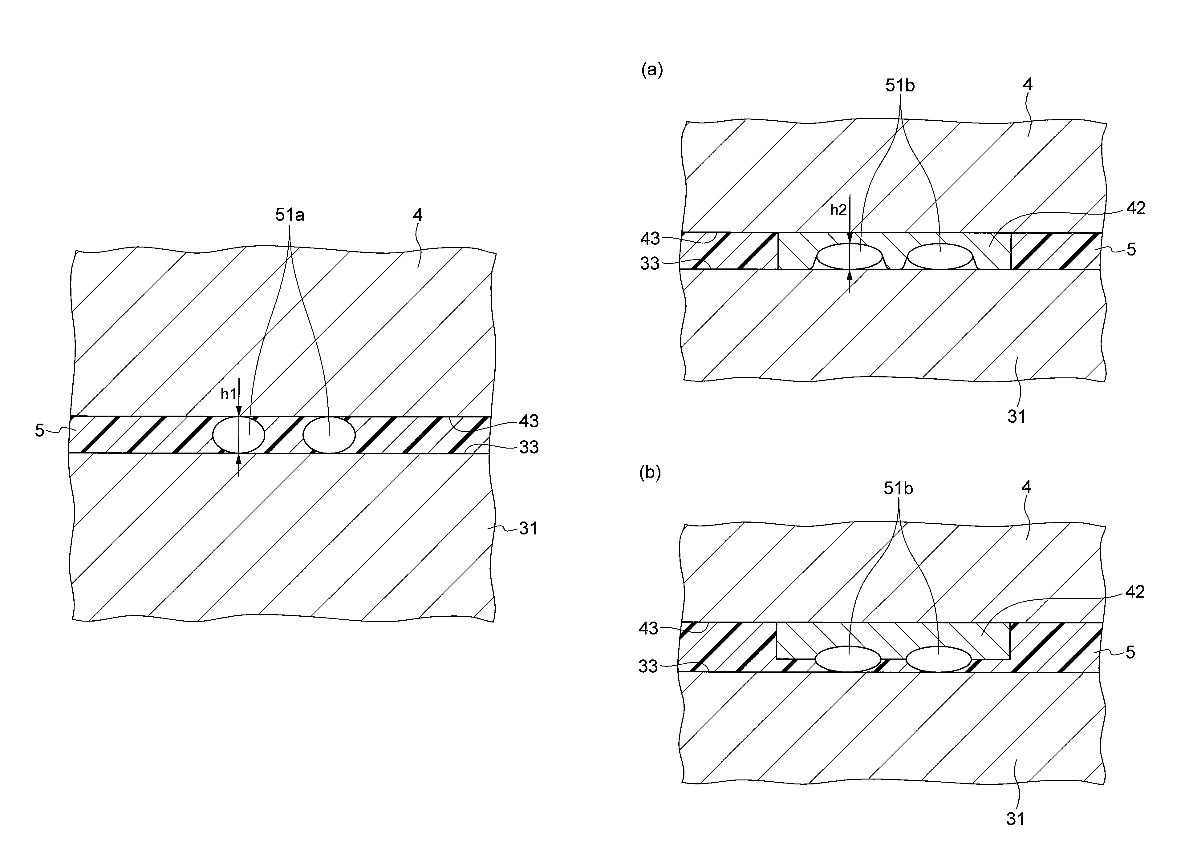
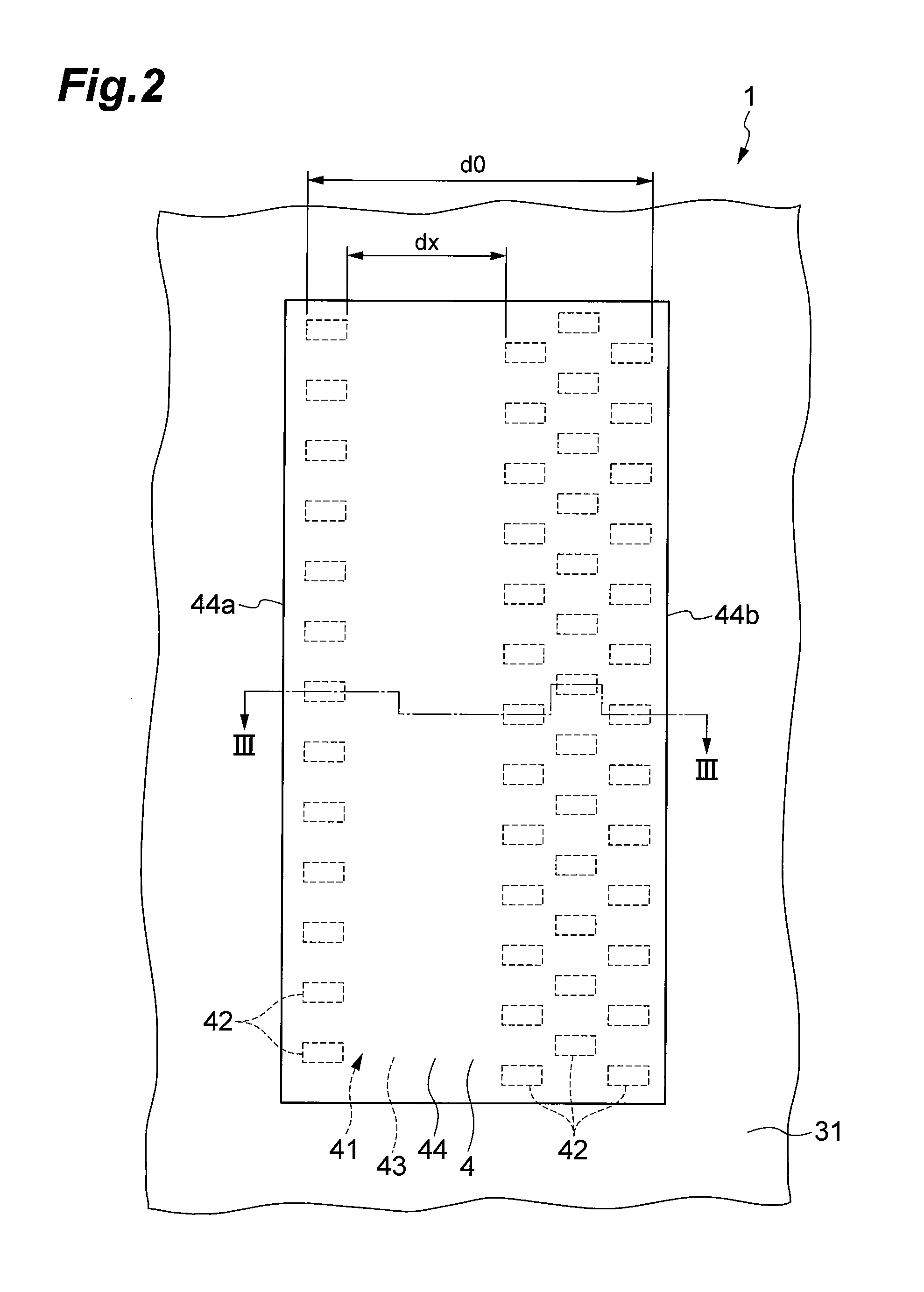
[0031]FIG. 1 is a plan view illustrating an electronic device to which the circuit component according to the embodiment is applied, FIG. 2 is a plan view illustrating the circuit component of FIG. 1, and FIG. 3 is a schematic cross-sectional view taken by an arrow III-III in FIG. 2. Note that, in FIG. 3, electrically conductive particles contained in an electrically conductive adhesive 5 to be described later are omitted.

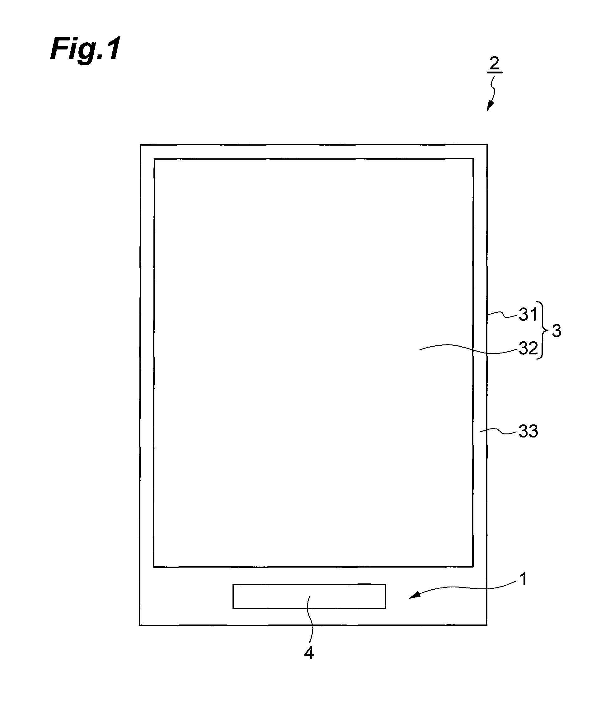
[0032]As illustrated in FIG. 1, a circuit component 1 is applied to, for example, an electronic device 2 such as a touch panel. The electronic device 2 includes a liquid crystal panel 3 and an IC chip 4.

[0033]The liquid crystal panel 3 includes a glass substrate 31 and a liquid crystal display part 32. The glass substrate 31 has a rectangular plate-like shape, a...


PUM


Abstract

The present invention provides a circuit component that enables satisfactory connection between a substrate and an IC chip and a method of making the same. The circuit component includes an IC chip and a substrate connected to each other using an electrically conductive adhesive containing electrically conductive particles. Bump electrodes and a non-electrode surface are provided on a mounting surface of the IC chip. The non-electrode surface is a portion of the mounting surface other than a portion where the bump electrodes are formed. Electrically conductive particles are placed in a first state between the surfaces of the substrate and the non-electrode surface so as to be in contact with both surfaces. Electrically conductive particles are placed in a second state between the surfaces of both the substrate and the bump electrodes, so as to be more flattened than the first state and dig into the bump electrodes.

Description

[0001]This application claims priority from Japanese Patent Application No. P2011-235145, filed Oct. 26, 2011, the entire disclosure of which is incorporated herein by reference.BACKGROUND OF THE INVENTION[0002]1. Field of the Invention[0003]The present invention relates to a circuit component and a method of making the same.[0004]2. Related Background Art[0005]When a circuit component is made by connecting a substrate such as a glass panel for liquid crystal display and an IC chip such as an IC for liquid crystal driving to each other, an electrically conductive adhesive containing electrically conductive particles may be used in some cases. In the case where the electrically conductive adhesive is used to make the circuit component, a plurality of bump electrodes provided to the IC chip can be connected to the substrate at a time. For example, according to Japanese Patent Laid-Open No. 2010-251789, an LCD panel and an IC chip are joined to each other using an anisotropic conductiv...

Claims


Application Information

Patent Timeline
Patent Type & Authority Patents(United States)
IPC IPC(8): H05K1/11H01L23/00H05K1/03H05K3/32H05K3/34
CPCH05K1/11H01L24/81H05K3/323H01L24/29H01L24/73H01L24/83H05K1/0306H05K3/3436H01L2224/29384H01L2224/2939H01L2224/29455H01L2224/29439H01L2224/29447H01L2224/2932H01L24/13H01L24/16H01L2224/13144H01L2224/16225H01L2224/2929H01L2224/29311H01L2224/29339H01L2224/29344H01L2224/29347H01L2224/29355H01L2224/29369H01L2224/29387H01L2224/29388H01L2224/29393H01L2224/29411H01L2224/73204H01L2224/81203H01L2224/81345H01L2224/81409H01L2224/83192H01L2924/10253H01L2924/14H01L2924/15788H01L2924/3511H01L2224/29444H01L2224/29469H01L2224/29493H01L2224/2942H01L2224/29484H01L2924/15787H01L2924/00H01B1/22H01B5/16H01B13/00H05K1/14
Inventor SATO, KAZUYA
Owner RESONAC CORPORATION
Why Eureka
Try Eureka