Group III nitride semiconductor light-emitting device and method for producing the same

a technology of nitride semiconductors and light-emitting devices, which is applied in the direction of semiconductor devices, basic electric elements, electrical equipment, etc., can solve the problem that the effect of relaxing the strain cannot be reached to a maximum extent, and achieve the effect of high light emission efficiency

Active Publication Date: 2015-05-12
TOYODA GOSEI CO LTD
View PDF4 Cites 2 Cited by
  • Summary
  • Abstract
  • Description
  • Claims
  • Application Information

AI Technical Summary

Benefits of technology

[0011]In the Group III nitride semiconductor light-emitting device, the strain applied to the light-emitting layer is relaxed. The pit-provided underlying layer, and the superlattice layer formed on the underlying layer appropriately absorb strain. As a result, the strain applied to the light-emitting layer is relaxed. Thus, the intensity of the piezoelectric field generated in the light-emitting layer is smaller than that of a conventional semiconductor light-emitting device. That is, the light emission efficiency of the Group III nitride semiconductor light-emitting device is higher than that of a conventional semiconductor light-emitting device.
[0014]A fourth aspect of the present invention is drawn to a specific embodiment of the Group III nitride semiconductor light-emitting device, wherein the underlying layer is an electrostatic-breakdown-voltage-improving layer for preventing electrostatic breakdown of each semiconductor layer.
[0022]Through employment of the method for producing a Group III nitride semiconductor light-emitting device, the strain propagating from a nitride semiconductor template—a layer under the underlying layer—can be efficiently relaxed, whereby the strain applied to the light-emitting layer can be reduced. In addition, the crystallinity of the formed semiconductor layers is maintained, and the portions of the semiconductor layers other than pit-provided regions have high flatness. Therefore, the formed light-emitting layer has high crystallinity. In other words, a Group III nitride semiconductor light-emitting device having high light emission efficiency can be produced. In the thus-produced Group III nitride semiconductor light-emitting device, the strain applied to the light-emitting layer is relaxed, since the pit-provided underlying layer, and the superlattice layer disposed on the underlying layer suitably absorb the strain. Thus, the strain applied to the light-emitting layer can be reduced, and the effect of a piezoelectric field on the light-emitting layer is reduced.
[0025]The present invention enables provision of a Group III nitride semiconductor light-emitting device in which the strain applied to the light-emitting layer is relaxed, to thereby attain high light emission efficiency, and a production method therefor.

Problems solved by technology

However, even when a superlattice layer is simply combined with an electrostatic-breakdown-voltage-improving layer, the two layers being formed so as to relax the strain to a maximum extent, the effect of relaxing the strain cannot be attained to a maximum extent.

Method used


Image

  • Group III nitride semiconductor light-emitting device and method for producing the same
  • Group III nitride semiconductor light-emitting device and method for producing the same
  • Group III nitride semiconductor light-emitting device and method for producing the same

Examples


Embodiment Construction

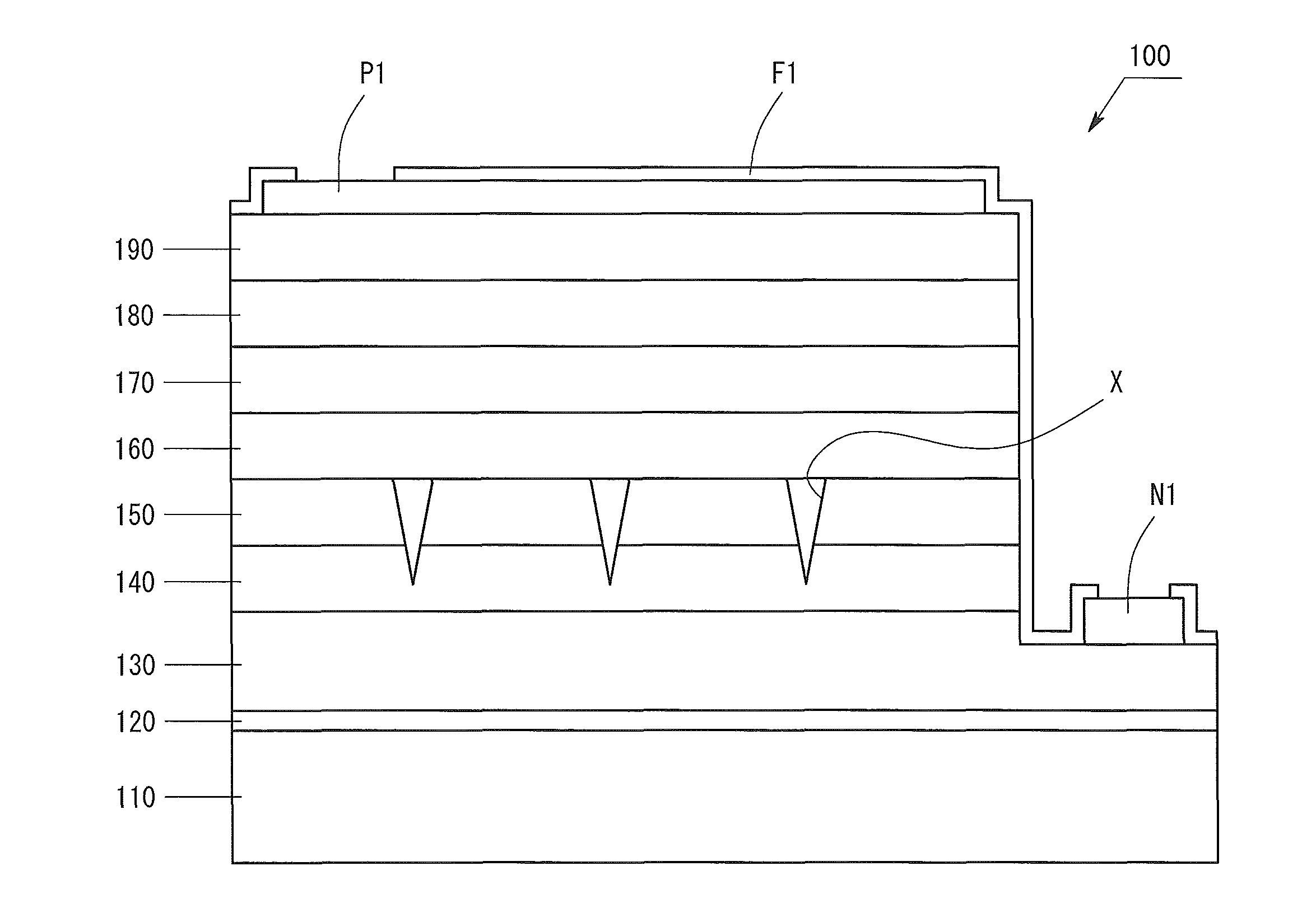
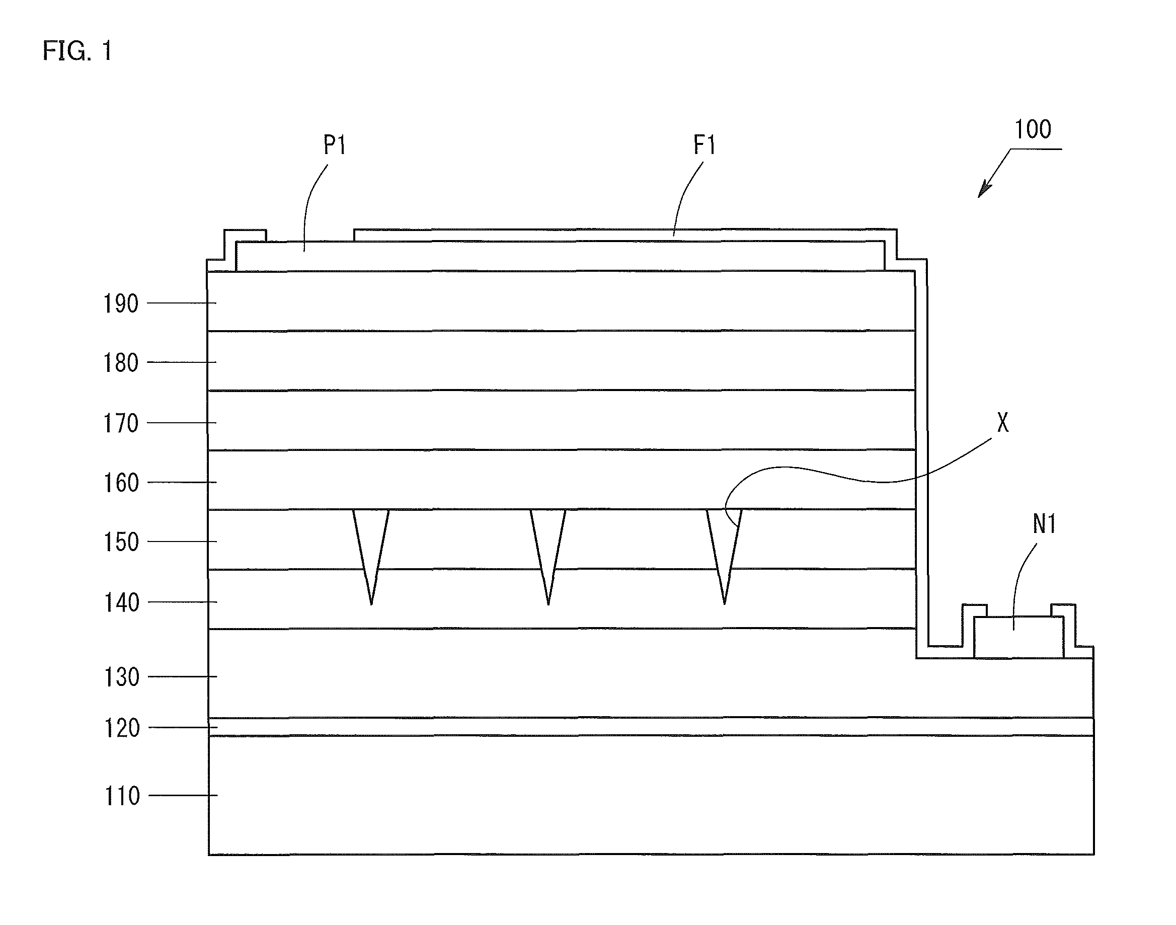
[0036]Specific embodiments of the present invention will next be described with reference to the drawings by taking, as an example, the case where a semiconductor light-emitting device is produced. However, the present invention is not limited to the embodiments. Needless to say, the structures of the layers and electrodes forming the below-mentioned light-emitting devices are merely examples, and may differ from those exemplified in the below-described embodiments. The thickness of each layer, which is schematically shown in the drawings, does not correspond to its actual value. Also, the dimensions of the pits shown in the drawings are larger than the actual values.

1. SEMICONDUCTOR LIGHT-EMITTING DEVICE

[0037]FIG. 1 is a schematic view of the structure of a Group III nitride semiconductor light-emitting device 100 according to the present embodiment. As shown in FIG. 1, the light-emitting device 100 is a face-up-type semiconductor light-emitting device. The light-emitting device 10...


PUM


Abstract

The invention provides a Group III nitride semiconductor light-emitting device in which the strain in the light-emitting layer is relaxed, thereby attaining high light emission efficiency, and a method for producing the device. The light-emitting device of the present invention has a substrate, a low-temperature buffer layer, an n-type contact layer, a first ESD layer, a second ESD layer, an n-side superlattice layer, a light-emitting layer, a p-side superlattice layer, a p-type contact layer, an n-type electrode N1, a p-type electrode P1, and a passivation film F1. The second ESD layer has pits X having a mean pit diameter D. The mean pit diameter D is 500 Å to 3,000 Å. An InGaN layer included in the n-side superlattice layer has a thickness Y satisfying the following condition: −0.029×D+82.8≦Y≦−0.029×D+102.8.

Description

BACKGROUND OF THE INVENTION[0001]1. Field of the Invention[0002]The present invention relates to a Group III nitride semiconductor light-emitting device and to a method for producing the same. More particularly, the present invention relates to a Group III nitride semiconductor light-emitting device in which strain applied to the light-emitting layer is relaxed, and to a method for producing the same.[0003]2. Background Art[0004]Generally, Group III nitride semiconductor light-emitting devices are produced through epitaxial growth of a Group III nitride semiconductor from a growth substrate. In this process, a plurality of Group III nitride semiconductor layers having different lattice constants are formed. Due to the lattice constant difference, strain (i.e., stress) generates in a relevant semiconductor layer. The stress generates a piezoelectric field, which deforms the potential of the quantum well of the light-emitting layer, thereby spatially separating electrons from holes. A...

Claims


Application Information

Patent Timeline
Patent Type & Authority Patents(United States)
IPC IPC(8): H01L29/06H01L33/02H01L33/06H01L33/32
CPCH01L33/02H01L33/06H01L33/32
Inventor OKUNO, KOJIMIYAZAKI, ATSUSHI
Owner TOYODA GOSEI CO LTD
Why Eureka
Try Eureka