Process variability tolerant hard mask for replacement metal gate finFET devices

a technology of hard mask and metal gate, which is applied in the direction of semiconductor devices, basic electric elements, electrical equipment, etc., can solve the problems of process challenges and device dimensions decreasing

Inactive Publication Date: 2015-05-19
INT BUSINESS MASCH CORP
View PDF11 Cites 12 Cited by
  • Summary
  • Abstract
  • Description
  • Claims
  • Application Information

AI Technical Summary

Problems solved by technology

Process challenges exist as the dimensions of the devices decrease.

Method used


Image

  • Process variability tolerant hard mask for replacement metal gate finFET devices
  • Process variability tolerant hard mask for replacement metal gate finFET devices
  • Process variability tolerant hard mask for replacement metal gate finFET devices

Examples


Embodiment Construction

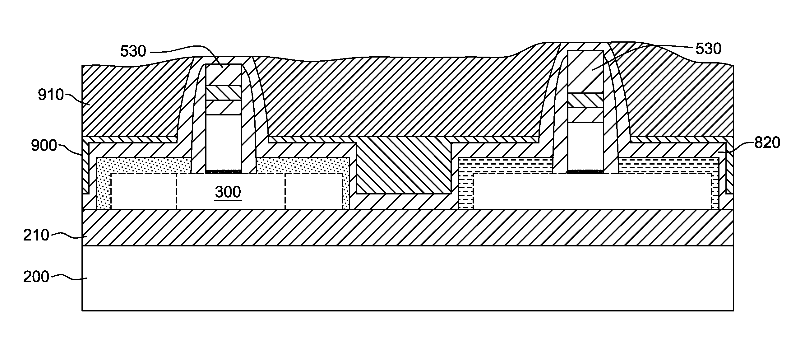
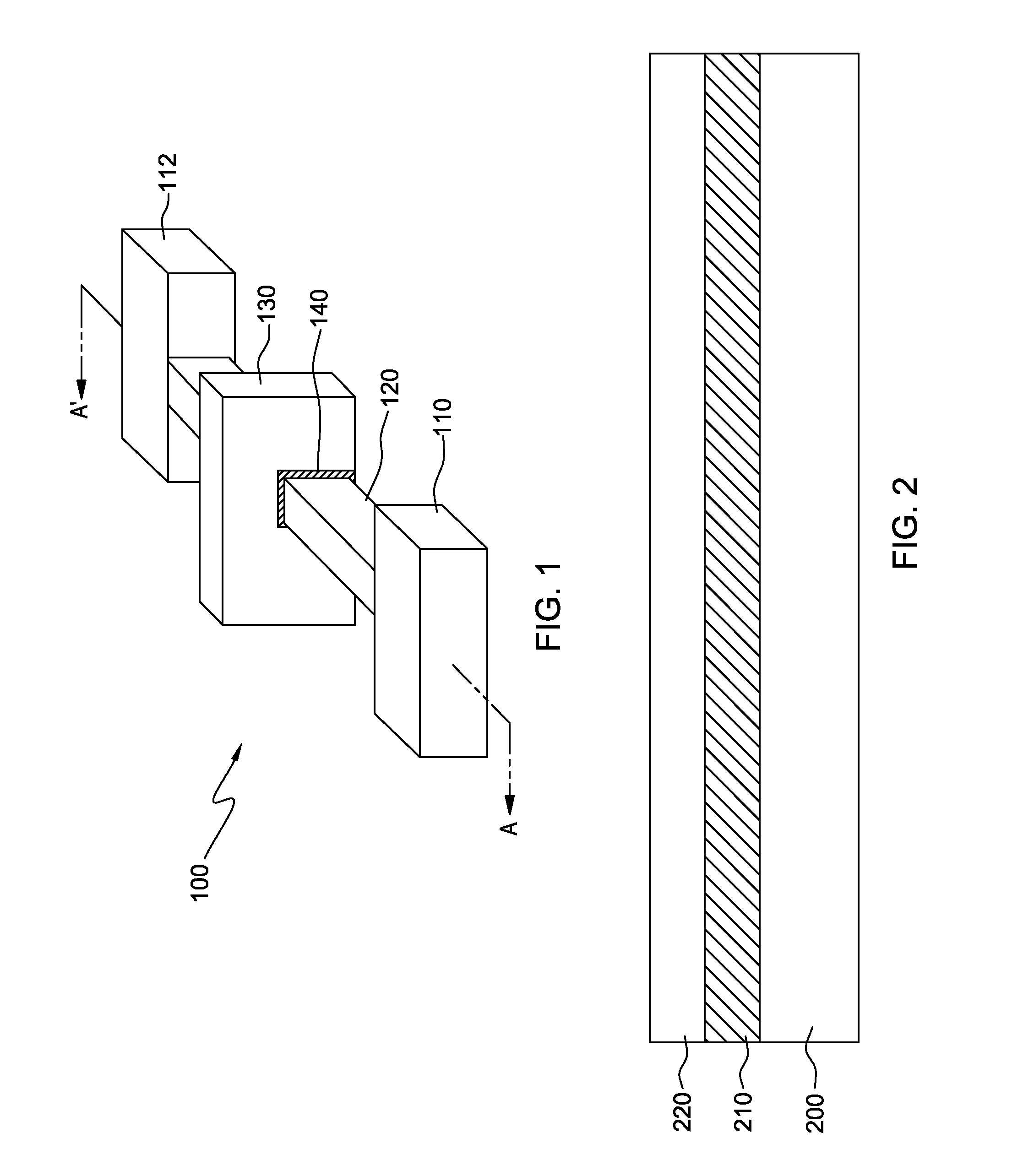
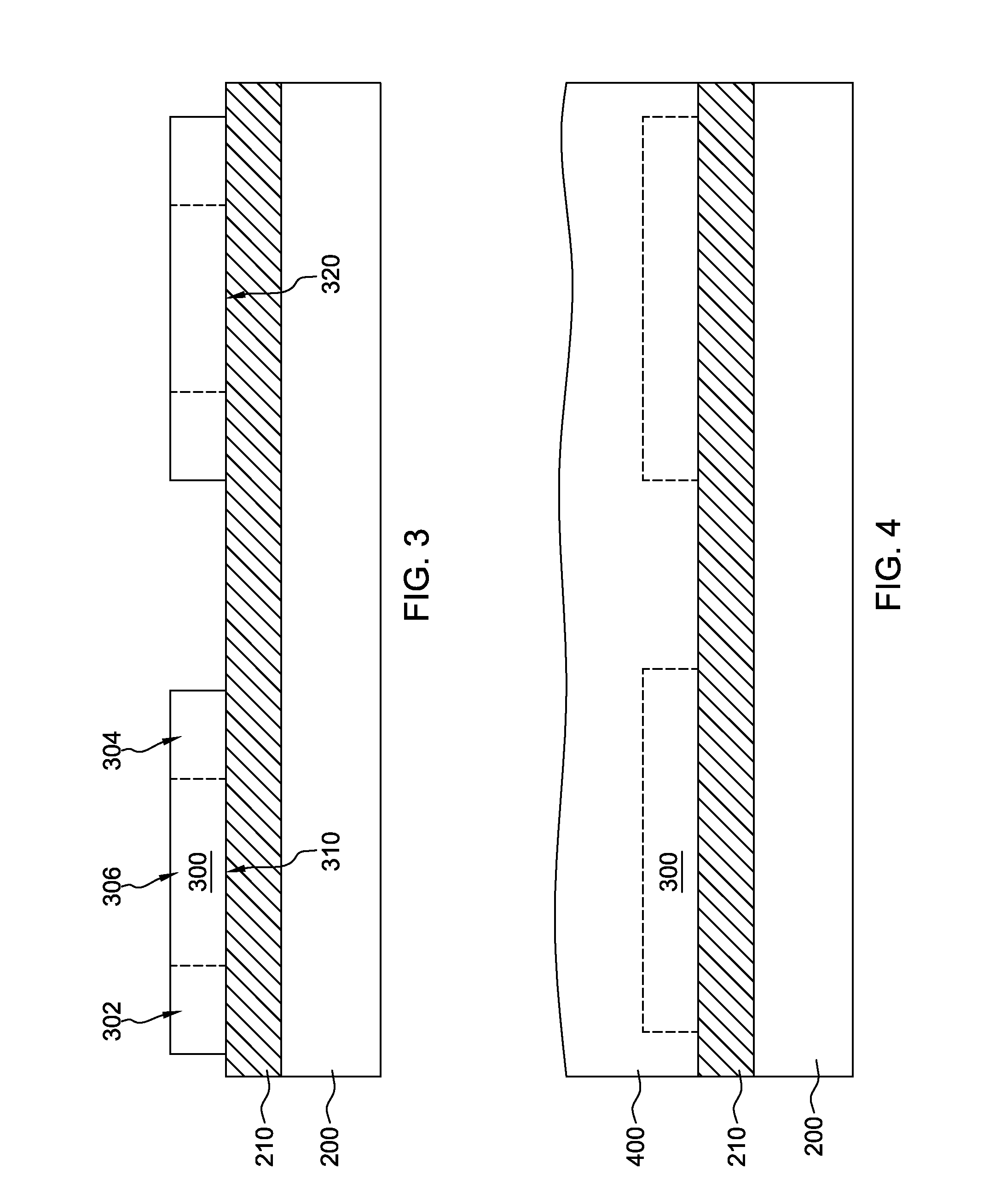
[0018]Embodiments of the present invention generally provide a process variability tolerant hard mask design for a RMG finFET device. Detailed description of embodiments of the claimed structures and methods are disclosed herein; however, it is to be understood that the disclosed embodiments are merely illustrative of the claimed structures and methods that may be embodied in various forms. In addition, each of the examples given in connection with the various embodiments is intended to be illustrative, and not restrictive. Further, the figures are not necessarily to scale, some features may be exaggerated to show details of particular components. Therefore, specific structural and functional details disclosed herein are not to be interpreted as limiting, but merely as a representative basis for teaching one skilled in the art to variously employ the methods and structures of the present disclosure.

[0019]References in the specification to “one embodiment”, “an embodiment”, “an examp...


PUM

PropertyMeasurementUnit
thickaaaaaaaaaa
thickaaaaaaaaaa
feature sizesaaaaaaaaaa

Abstract

Embodiments include a method comprising depositing a hard mask layer over a first layer, the hard mask layer including; lower hard mask layer, hard mask stop layer, and upper hard mask. The hard mask layer and the first layer are patterned and a spacer deposited on the patterned sidewall. The upper hard mask layer and top portion of the spacer are removed by selective etching with respect to the hard mask stop layer, the remaining spacer material extending to a first predetermined position on the sidewall. The hard mask stop layer is removed by selective etching with respect to the lower hard mask layer and spacer. The first hard mask layer and top portion of the spacer are removed by selectively etching the lower hard mask layer and the spacer with respect to the first layer, the remaining spacer material extending to a second predetermined position on the sidewall.

Description

FIELD OF THE INVENTION[0001]The present invention relates generally to the fabrication of semiconductor devices, and more particularly to the fabrication of a finFET device.BACKGROUND OF THE INVENTION[0002]Field effect transistors (FETs) can be semiconductor devices fabricated on a bulk semiconductor substrate or on a silicon-on-insulator (SOI) substrate. FET devices generally consist of a source, a drain, a gate, and a channel between the source and drain. The gate is separated from the channel by a thin insulating layer, typically of silicon oxide, called the field or gate oxide. A voltage drop generated by the gate across the oxide layer induces a conducting channel between the source and drain thereby controlling the current flow between the source and the drain. Current integrated circuit designs use complementary metal-oxide-semiconductor (CMOS) technology that use complementary and symmetrical pairs of p-type and n-type metal oxide semiconductor field effect transistors (MOSF...

Claims


Application Information

Patent Timeline
Patent Type & Authority Patents(United States)
IPC IPC(8): H01L21/302H01L21/461H01L21/033H01L21/28H01L21/3213H01L29/66
CPCH01L21/28132H01L29/6681H01L21/0332H01L21/32139Y10S438/95H01L21/31055H01L21/31116H01L21/31144H01L21/823814H01L21/823821H01L21/845H01L29/66545
Inventor BAIOCCO, CHRISTOPHER V.CHAN, KEVIN K.KIM, YOUNG-HEEKOBAYASHI, MASAHARULEOBANDUNG, EFFENDILIU, FEIPARK, DAE-GYUWANG, HELENWANG, XINHUIYANG, MIN
Owner INT BUSINESS MASCH CORP
Why Eureka
Try Eureka