Energy conditioning circuit arrangement for integrated circuit

a technology of energy conditioning circuit and integrated circuit, which is applied in the direction of emergency protective arrangements for limiting excess voltage/current, cross-talk/noise/interference reduction, and electrical systems that have undergone short product life cycles, etc., to achieve cost-effective and solve or reduce industry problems and obstacles

Inactive Publication Date: 2015-06-09
X2Y ATTENUATORS L L C
View PDF1067 Cites 39 Cited by
  • Summary
  • Abstract
  • Description
  • Claims
  • Application Information

AI Technical Summary

Benefits of technology

[0020]The invention will also provide for simultaneous physical and electrical shielding to portions of an active chip structure as well as for internal propagating energies within the new structure by allowing predetermined, simultaneous energy interactions to take place between grouped and energized conductive pathways to be fed by pathways external to the embodiment elements.
[0021]This application expands upon this concept and further discloses a new circuit interposer comprising a multilayer, universal multi-functional, common conductive shield structure with conductive pathways that replaces multiple, discreet versions of various prior art devices with a single individual unit that provides a cost effective system of circuit protection and conditioning that will help solve or reduce industry problems and obstacles as described above.
[0024]It is an object of the invention to minimize or suppress unwanted electromagnetic emissions resulting from differential and common mode currents flowing within electronic pathways that come under the invention influence.
[0027]It is an object of the invention to be easily adapted to utilization with or without, one or more external conductive attachments to a conductive area located external to the originally manufactured invention. The external connection to a conductive area—can aid the invention embodiments in providing protection to electronic system circuitry.

Problems solved by technology

A main disadvantage of conventional approaches to interconnecting and packaging of IC chips in Multi Chip Modules (MCMs) arises from the thinness of the substrates used in traditional multichip modules results in the energy feeds to the IC chips having relatively high impedance.
This results in undesired noise, energy loss and excess thermal energy production.
These problems are relevant and can be critical to system integrity when routing or propagating energy along pathways though an interposer substrate.
Electrical systems have undergone short product life cycles over the last decade.
However, the evolvement of passive electronic componentry has not kept pace.
During this same period, however, passive component technologies have failed to keep up with these new breakthroughs and have produced only incremental changes in composition and performance.
Attempts to line condition propagating energy with prior art components has led to increased levels of interference in the form of EMI, RFI, and capacitive and inductive parasitics.
These increases are due in part to manufacturing imbalances and performance deficiencies of the passive components that create or induce interference into the associated electrical circuitry.
Other sources of EMI interference are generated from the active silicon components as they operate or switch.
These problems such as SSO are notorious causes of circuit disruptions.
Other problems include unshielded and parasitic energy that freely couples upon or onto the electrical circuitry and generates significant interference at high frequencies.

Method used


Image

  • Energy conditioning circuit arrangement for integrated circuit
  • Energy conditioning circuit arrangement for integrated circuit
  • Energy conditioning circuit arrangement for integrated circuit

Examples


embodiment 20

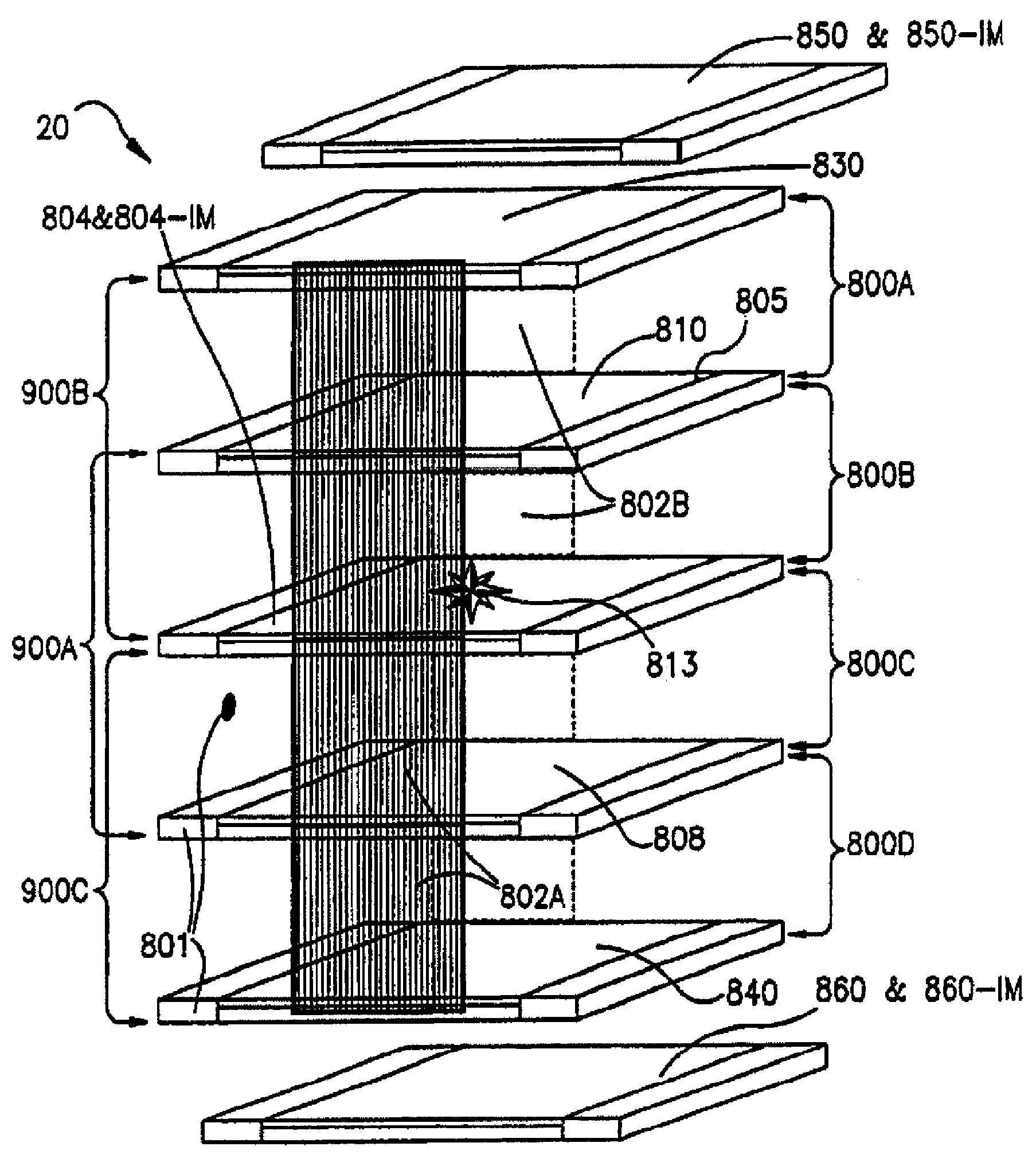
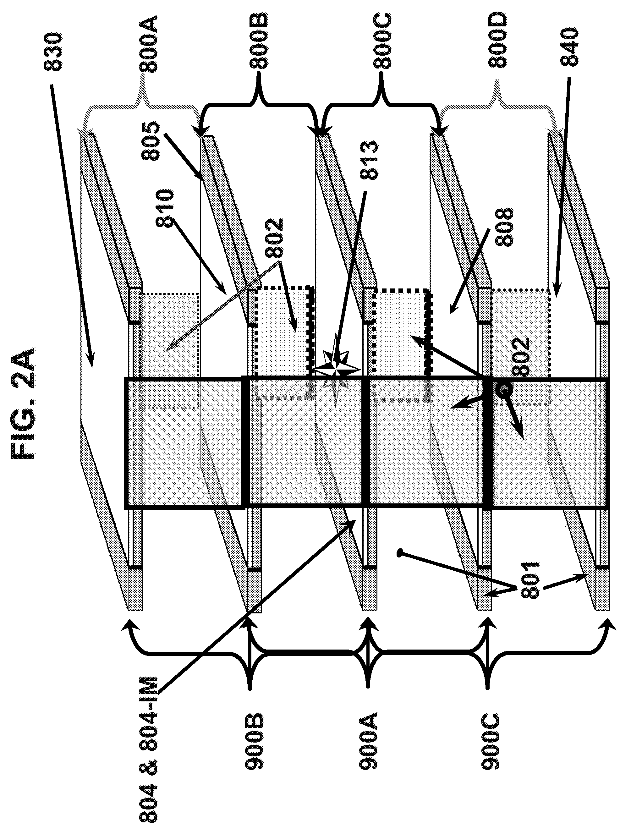
[0130]Before embodiment 20 of FIG. 4 is placed into circuitry and energized, structures 802A and 802B should electrically connect conductive pathways to one another in a typical circuit system and provide externally located conductive pathways or areas (not shown) or same external conductive paths (not shown) a good electrical connection without any conductive interruption or gap between each respective conductive structures 802A and 802B.

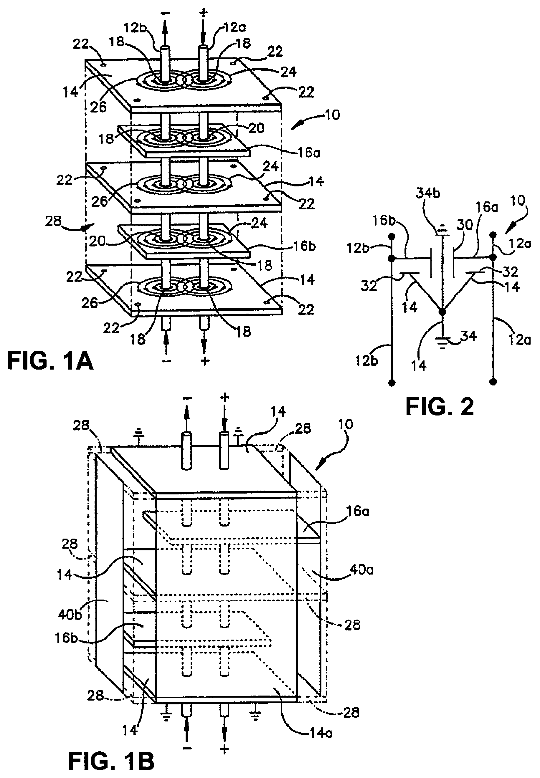
[0131]In FIG. 3, single cage-like structure 800B mirrors single cage-like structure 800C except that differential electrode 818 (not shown) contained within, and exit / entrance sections 812A and 812B (not shown) as well as conductive pathway extension structures 812A and 812B (not shown), are positioned in a generally opposite placement position relative to one another or its paired mate in multi-paired applications, and will operate in an electrically balanced manner with one another conductive pathway differential electrode of conductive structure...


PUM


Abstract

The present invention relates to an interposer substrate for interconnecting between active electronic componentry such as but not limited to a single or multiple integrated circuit chips in either a single or a combination and elements that could comprise of a mounting substrate, substrate module, a printed circuit board, integrated circuit chips or other substrates containing conductive energy pathways that service an energy utilizing load and leading to and from an energy source. The interposer will also possess a multi-layer, universal multi-functional, common conductive shield structure with conductive pathways for energy and EMI conditioning and protection that also comprise a commonly shared and centrally positioned conductive pathway or electrode of the structure that can simultaneously shield and allow smooth energy interaction between grouped and energized conductive pathway electrodes containing a circuit architecture for energy conditioning as it relates to integrated circuit device packaging. The invention can be employed between an active electronic component and a multilayer circuit card. A method for making the interposer is not presented and can be varied to the individual or proprietary construction methodologies that exist or will be developed.

Description

CROSS REFERENCE TO RELATED APPLICATIONS[0001]This application is a continuation of application Ser. No. 12 / 795,625, filed Jun. 7, 2010, which is a continuation of application Ser. No. 12 / 567,777, filed Sep. 27, 2009, now issued as U.S. Pat. No. 7,733,621, which is a continuation of application Ser. No. 12 / 017,020, filed Jan. 19, 2008, now issued as U.S. Pat. No. 7,609,501, which is a continuation of application Ser. No. 11 / 828,522, filed Jul. 26, 2007, now issued as U.S. Pat. No. 7,609,500, which is a continuation of application Ser. No. 11 / 169,926, filed Jun. 30, 2005, now U.S. Pat. No. 7,301,748, which is a continuation of application Ser. No. 10 / 237,079, filed Sep. 9, 2002, now issued as U.S. Pat. No. 7,110,227, which is a continuation-in-part of application Ser. No. 09 / 632,048, filed Aug. 3, 2000, now issued as U.S. Pat. No. 6,738,249, which is a continuation-in-part of application Ser. No. 09 / 594,447, filed Jun. 15, 2000, now issued as U.S. Pat. No. 6,636,406, which is a contin...

Claims


Application Information

Patent Timeline
Patent Type & Authority Patents(United States)
IPC IPC(8): H02H9/00H01L23/498H01L23/552H01L23/60H03H1/00H05K1/02
CPCH01L23/49822H01L23/49827H01L23/552H01L23/60H03H1/0007H05K1/0233H01L2224/16227H01L2924/01322H01L2924/15311H01L2924/10253H01L2224/16225H01L2924/00H01L2224/05573H01L2224/05568H01L2924/00014H01L2224/05599
Inventor ANTHONY, ANTHONY A.ANTHONY, WILLIAM M.
Owner X2Y ATTENUATORS L L C
Why Eureka
Try Eureka