

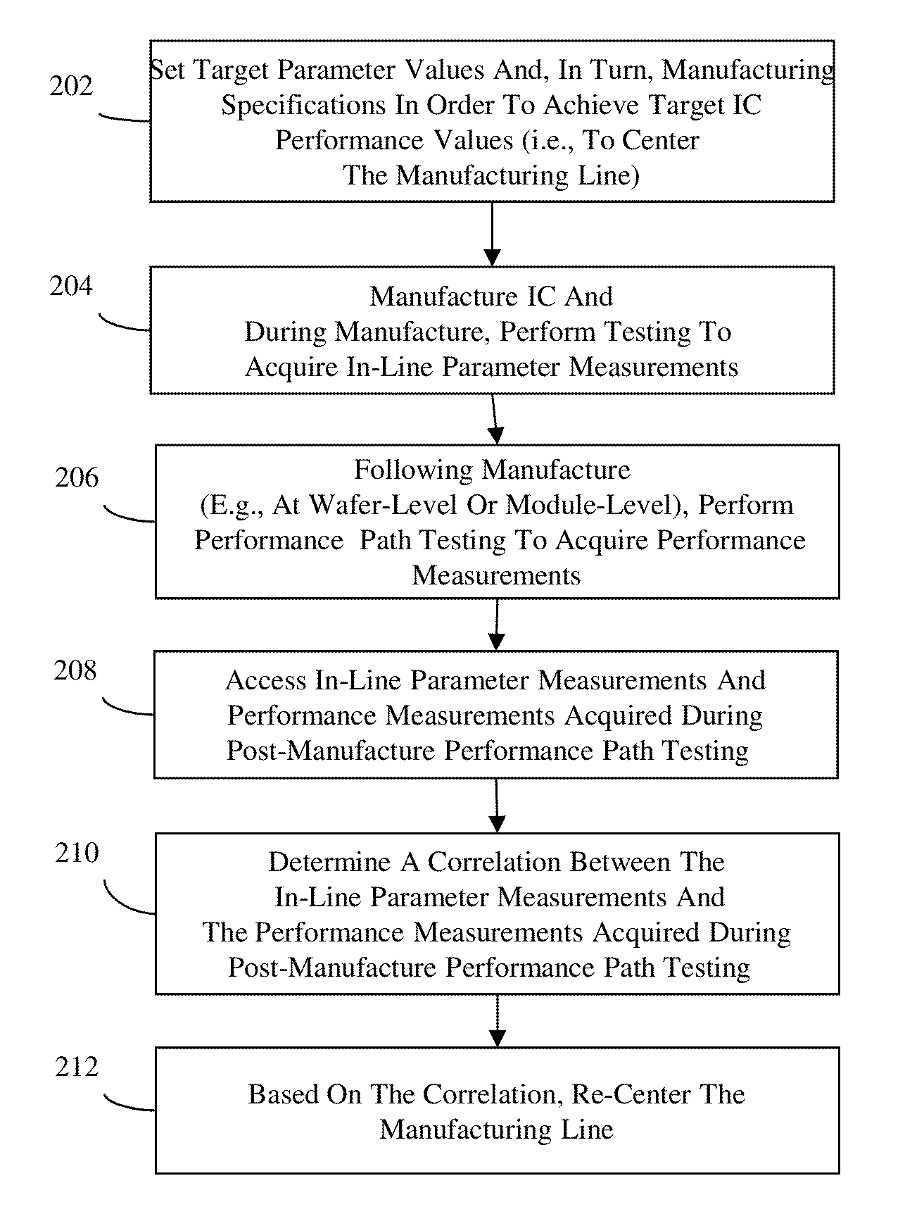
Integrated circuit product yield optimization using the results of performance path testing
a technology of integrated circuit and product yield, applied in the direction of instrumentation, programme control, total factory control, etc., can solve the problem of significant yield loss, achieve the effect of optimizing the yield of integrated circuit products, minimizing yield loss, and minimizing yield loss
- Summary
- Abstract
- Description
- Claims
- Application Information
AI Technical Summary
Benefits of technology
Problems solved by technology
Method used
Image

Examples
Embodiment Construction
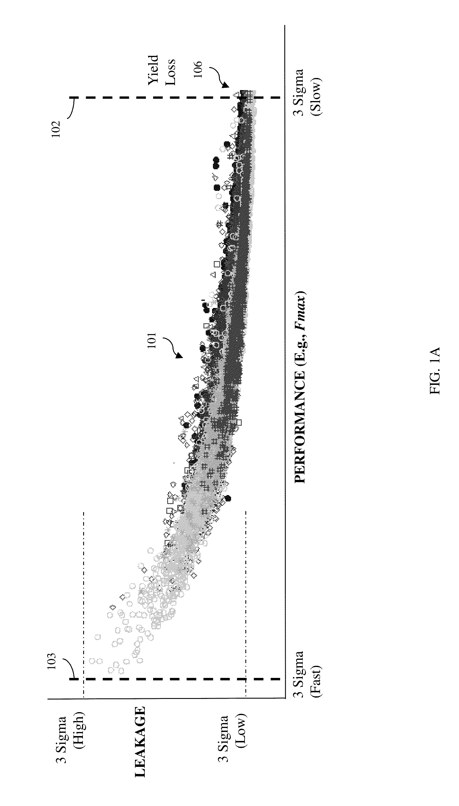
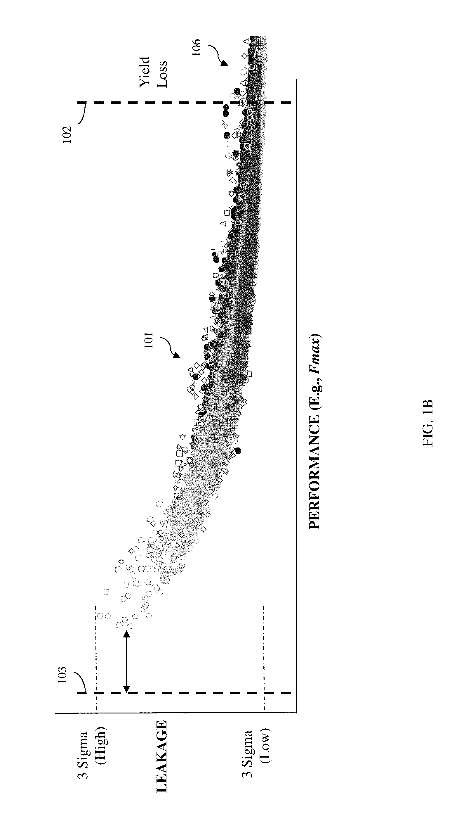
[0020]As mentioned above, currently, performance measurements and, particularly, frequency measurements acquired during performance screen ring oscillator (PSRO) testing are often used to disposition (i.e., screen) chips at both the wafer-level and the module-level (i.e., the integrated circuit chip package-level). For purposes of this disclosure, wafer-level chip dispositioning refers to wafer-level performance testing to determine whether the chips on wafers pass and, thus, are processed into chip modules or fail and, thus, are scrapped. Similarly, module-level chip dispositioning refers to module-level performance testing to determine whether the chip modules pass and, thus, are shipped to customers or fail and, thus, are scrapped. Performance measurements acquired during post-manufacture (i.e., wafer-level or module-level) PSRO testing are also often used as feedback to control or re-center (i.e., re-calibrate) the manufacturing line in order to account for product-to-product la...
PUM
 Abstract
Description
Claims
Application Information