Nitridation of atomic layer deposited high-k dielectrics using trisilylamine

a technology of trisilylamine and atomic layer, which is applied in the direction of coating, semiconductor devices, chemical vapor deposition coating, etc., can solve the problems of difficult insertion of nitrogen into high-k films

Active Publication Date: 2015-06-23
AIR LIQUIDE AMERICA INC +1
View PDF10 Cites 1 Cited by
  • Summary
  • Abstract
  • Description
  • Claims
  • Application Information

AI Technical Summary

Problems solved by technology

However, incorporating nitrogen into the high-k films has turned out to be difficult and often requires the use of nitrogen-containing plasma that contain high energy charged species that can damage materials in the semiconductor device.

Method used


Image

  • Nitridation of atomic layer deposited high-k dielectrics using trisilylamine
  • Nitridation of atomic layer deposited high-k dielectrics using trisilylamine
  • Nitridation of atomic layer deposited high-k dielectrics using trisilylamine

Examples


Embodiment Construction

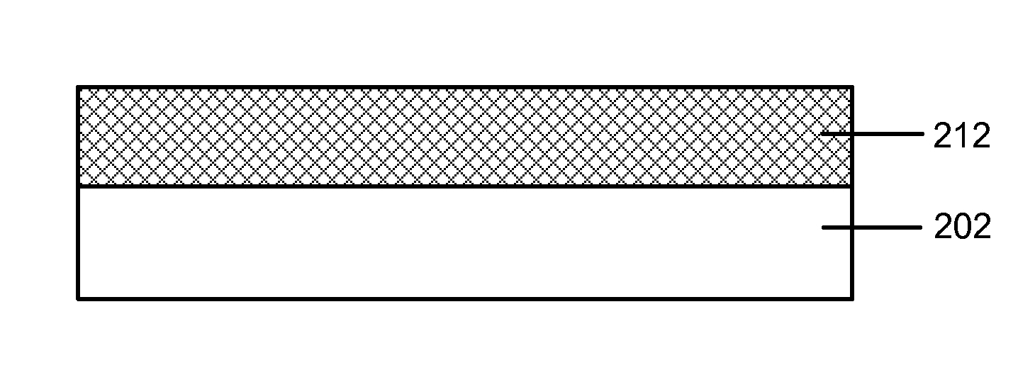
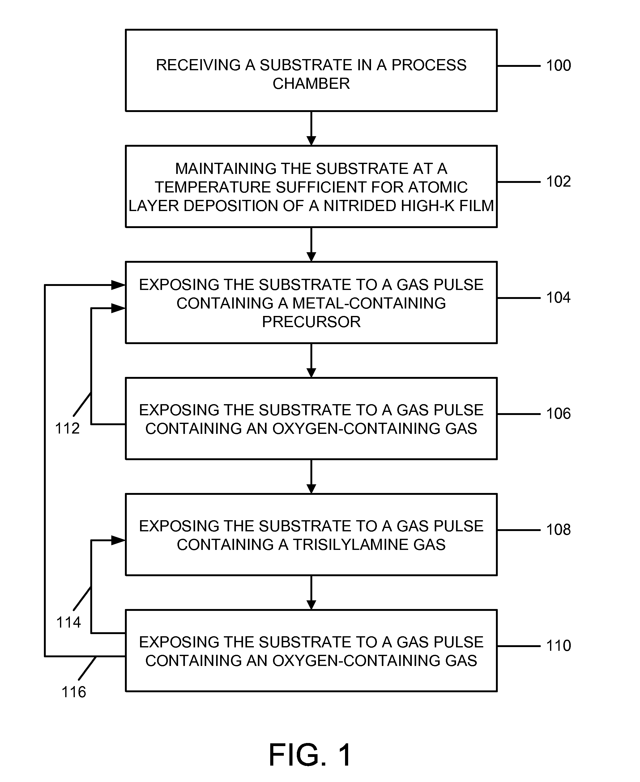
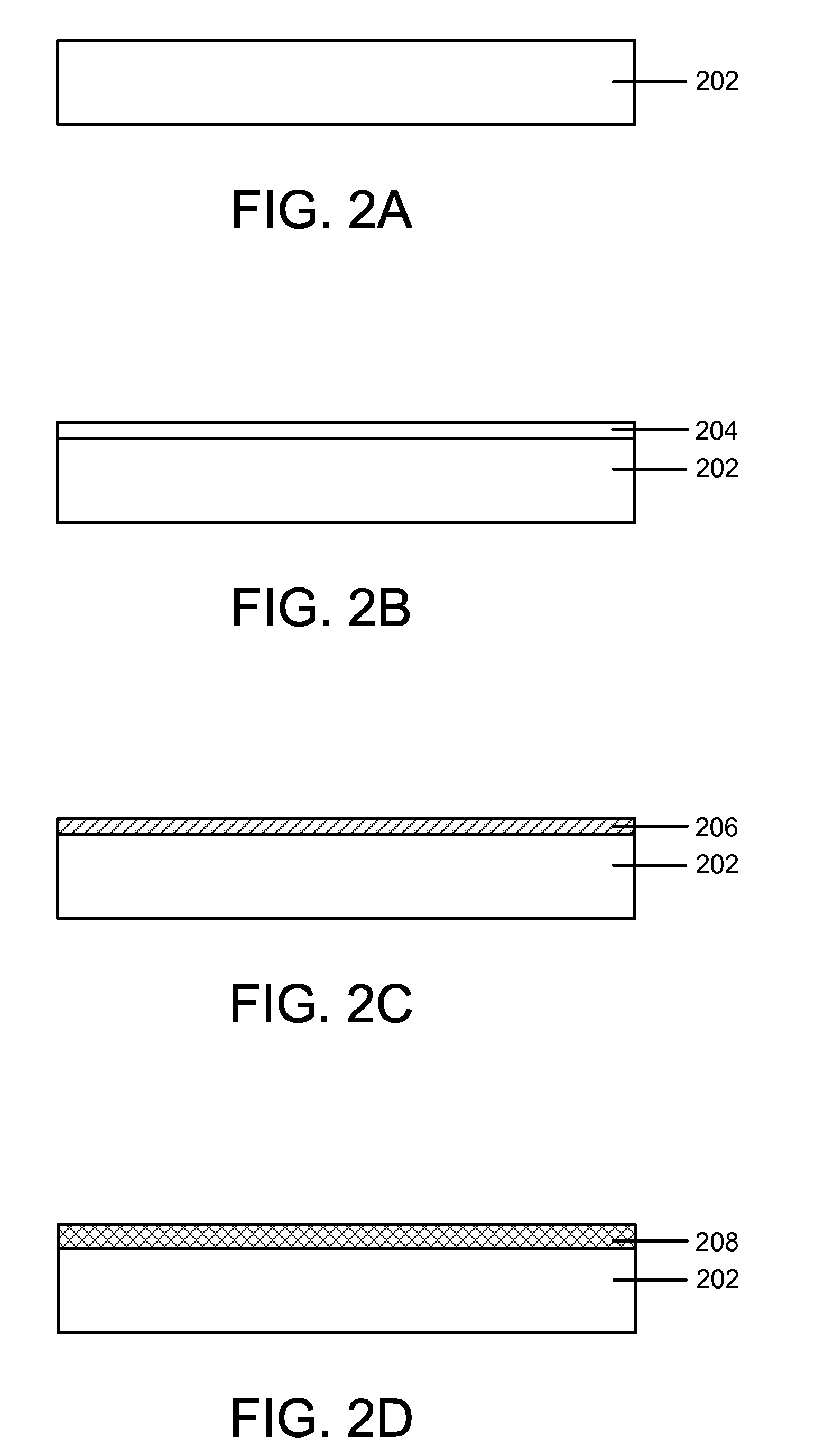
[0017]Methods for forming nitrided high-k films are disclosed in various embodiments. The current inventors have discovered an ALD process that efficiently incorporates nitrogen into a high-k film at a low substrate temperature in absence of a plasma. The process utilizes trisilylamine as a source of nitrogen for the nitrided high-k film but the process does not incorporate silicon into the nitrided high-k film. This is unexpected since chemical vapor deposition (CVD) using trisilylamine at higher substrate temperature incorporates both nitrogen and silicon into the high-k film. Benefits of nitridation can include a higher dielectric constant and improved diffusion barrier properties of the nitrided high-k film. In comparison, the presence of silicon in high-k films and nitrided high-k films has been shown to reduce the dielectric constant of the films and, therefore, it can be advantageous to avoid or limit the amount of silicon in high-k films for many semiconductor devices.

[0018]...


PUM

PropertyMeasurementUnit
physical thicknessaaaaaaaaaa
sizeaaaaaaaaaa
sizeaaaaaaaaaa

Abstract

A method is provided for forming a nitrided high-k film in an atomic layer deposition process (ALD) process. The method includes receiving a substrate in a process chamber, maintaining the substrate at a temperature sufficient for ALD of a nitrided high-k film, and depositing the nitrided high-k film on the substrate by exposing the substrate to a gas pulse sequence that includes, in any order: a) exposing the substrate to a gas pulse comprising a metal-containing precursor, b) exposing the substrate to a gas pulse comprising an oxygen-containing gas, and c) exposing the substrate to a gas pulse comprising trisilylamine gas, where the exposing the substrate to the trisilylamine gas yields the nitrided high-k film that includes nitrogen and that is substantially free of silicon, and repeating the gas pulse sequence. A trisilylamine gas exposure may also be used to nitride a deposited high-k film.

Description

CROSS-REFERENCE TO RELATED APPLICATION[0001]This application is related to and claims priority to U.S. Provisional application Ser. No. 61 / 670,737 filed on Jul. 12, 2012, the entire contents of which are herein incorporated by reference.FIELD OF INVENTION[0002]The present invention relates to the field of semiconductor manufacturing and more particularly to methods for forming nitrided high-k films for semiconductor devices.BACKGROUND OF THE INVENTION[0003]Recent advances in microelectronics have included the use of high-k films in gate dielectric stacks for logic applications. To increase device reliability and reduce electron leakage from the gate electrode to the transistor channel, semiconductor transistor technology is introducing high-k materials that allow increased physical thickness of the gate dielectric layer. Dielectric materials featuring a dielectric constant greater than that of SiO2 (k˜3.9) are commonly referred to as high-k materials. An early motivation for seeking...

Claims


Application Information

Patent Timeline
Patent Type & Authority Patents(United States)
IPC IPC(8): H01L21/02H01L29/51H01L21/28H01L21/469C23C16/00C23C16/30C23C16/455
CPCH01L21/02181H01L21/02189H01L21/02194H01L21/02148H01L21/02159H01L21/02161H01L21/0228H01L21/02326H01L21/02332H01L21/02337C23C16/308C23C16/45531H01L21/28194H01L29/518
Inventor CONSIGLIO, STEVEN PCLARK, ROBERT DDUSSARRAT, CHRISTIANOMARJEE, VINCENTPALLEM, VENKATKUCHENBEISER, GLENN
Owner AIR LIQUIDE AMERICA INC
Why Eureka
Try Eureka