Integrated circuit and method of forming integrated circuit

a technology of integrated circuits and integrated circuits, applied in the field of integrated circuits, to achieve the effect of reducing processing costs, saving a half space, and simplifying processes

Active Publication Date: 2015-06-23
MARLIN SEMICON LTD
View PDF13 Cites 14 Cited by
  • Summary
  • Abstract
  • Description
  • Claims
  • Application Information

AI Technical Summary

Benefits of technology

[0010]According to the above, the present invention provides an integrated circuit and a method thereof, which forms a patterned stacked structure including a bottom conductive layer, an insulating layer and a top conductive layer in a capacitor area and a resistor area by one single process, so that a capacitor in the capacitor area and a non...

Problems solved by technology

According to the above, how to integrate capacitors and resistors in a same semiconductor substrate...

Method used


Image

  • Integrated circuit and method of forming integrated circuit
  • Integrated circuit and method of forming integrated circuit
  • Integrated circuit and method of forming integrated circuit

Examples


Embodiment Construction

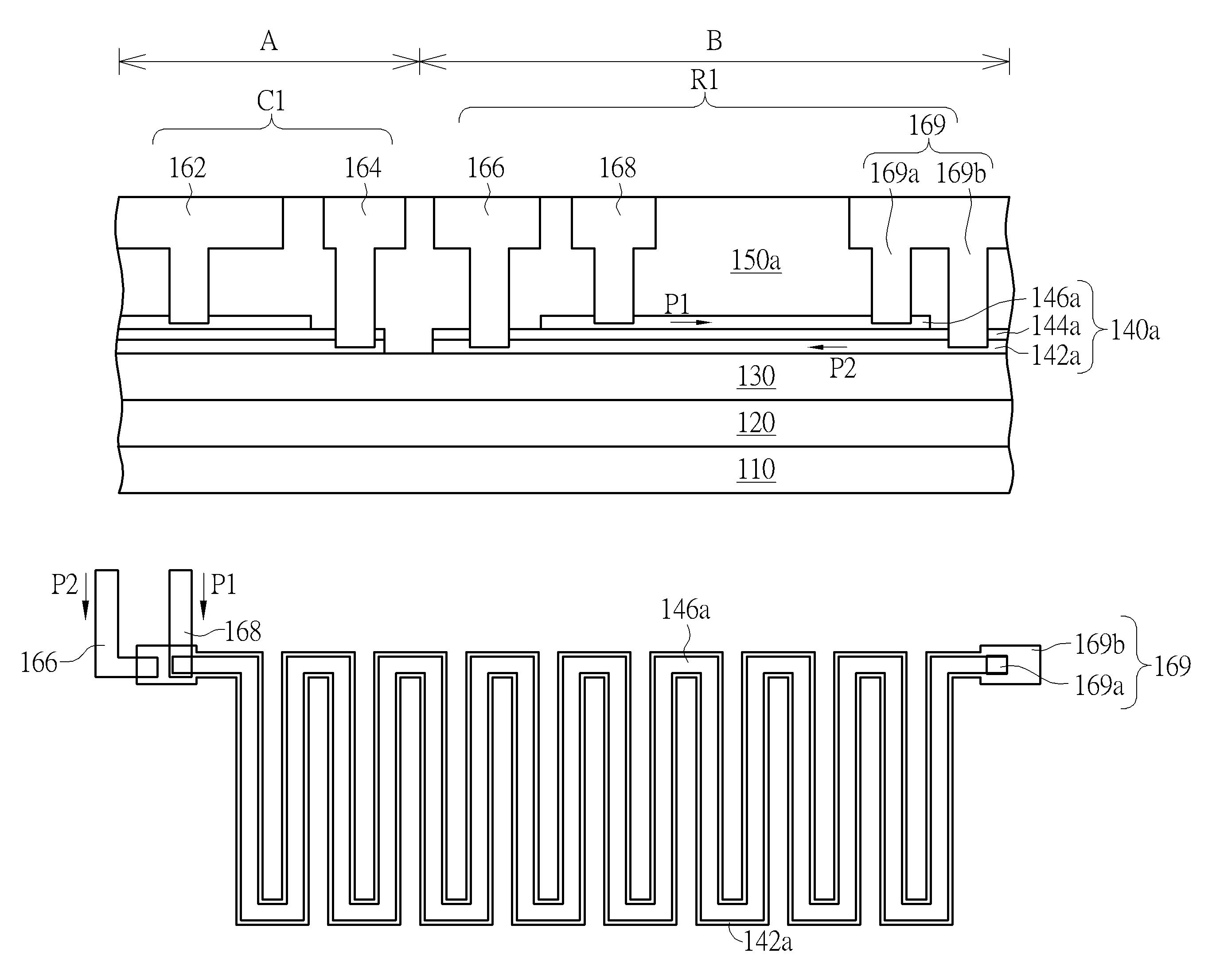
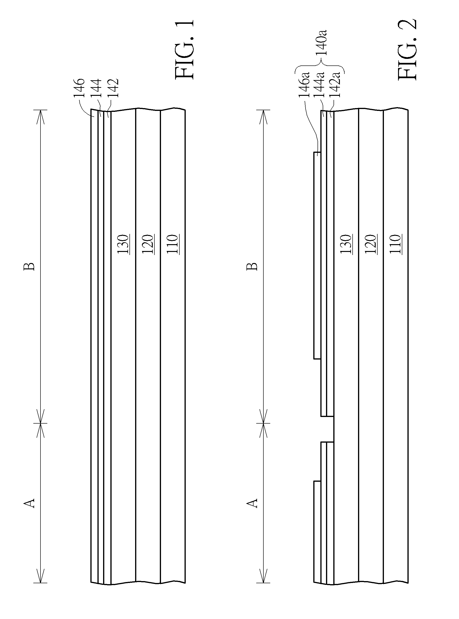
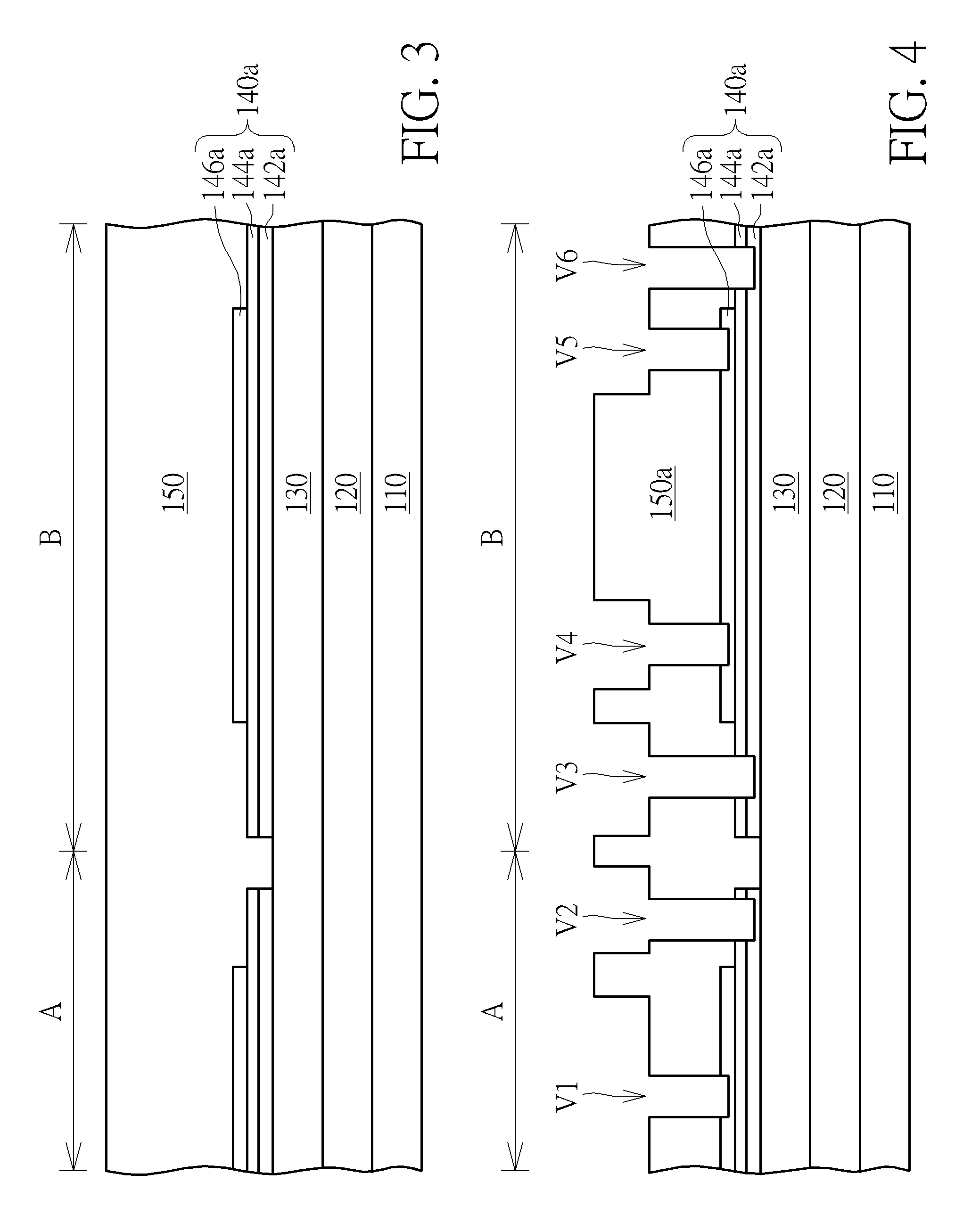
[0018]FIGS. 1-5 schematically depict cross-sectional views of an integrated circuit according to a first embodiment of the present invention. A substrate 110 including a capacitor area A and a resistor area B is provided. The substrate 110 may be a semiconductor substrate such as a silicon substrate, a silicon containing substrate, a III-V group-on-silicon (such as GaN-on-silicon) substrate, a graphene-on-silicon substrate or a silicon-on-insulator (SOI) substrate. In an embodiment, MOS transistors may be formed in or on the substrate 110. A first metal layer 120 may be formed on the substrate 110. In one embodiment, the first metal layer 120 is an interconnection structure, and the first metal layer 120 may be one layer of the multi-layers interconnection structure, but it is not limited thereto. More precisely, an interlevel dielectric layer (not shown) may be deposited on the substrate 110 by a thermal oxide process or a chemical oxide process etc., and then the interlevel dielec...


PUM


Abstract

An integrated circuit includes a capacitor and a non-inductive resistor. A substrate has a capacitor area and a resistor area. A patterned stacked structure including a bottom conductive layer, an insulating layer and a top conductive layer from bottom to top is sandwiched by a first dielectric layer and a second dielectric layer disposed on the substrate. A first metal plug and a second metal plug contact the top conductive layer and the bottom conductive layer of the capacitor area respectively, thereby the patterned stacked structure in the capacitor area constituting the capacitor. A third metal plug and a fourth metal plug contact the bottom conductive layer and the top conductive layer of the resistor area respectively, and a fifth metal plug contacts the bottom conductive layer and the top conductive layer of the resistor area simultaneously, thereby the patterned stacked structure in the resistor area constituting the non-inductive resistor.

Description

BACKGROUND OF THE INVENTION[0001]1. Field of the Invention[0002]The present invention relates generally to an integrated circuit and the manufacturing method thereof, and more specifically to an integrated circuit including a capacitor and a non-inductive resistor and the manufacturing method thereof.[0003]2. Description of the Prior Art[0004]Capacitors and resistors are widely used in digital circuits in current semiconductor industries. As the integration of electrical circuits increases, it becomes mainstream to form a semiconductor device by integrating transistors, capacitors and resistors into one same semiconductor substrate.[0005]In semiconductor processes, the operating theory of a capacitor is to set two electrode layers as a top and a bottom electrode plate in a semiconductor die, and an insulating layer separating the two electrode layers from a predetermined distance. As a voltage is applied on the two electrode layers, the capacitor is electrically charged. A metal cap...

Claims


Application Information

Patent Timeline
IPC IPC(8): H01L23/52H01L27/06H01L27/12
CPCH01L27/0688H01L27/1203H01L2224/48247H01L27/0629H01L27/0682
Inventor ZHOU, ZHIBIAOWU, SHAO-HUIKU, CHI-FA
Owner MARLIN SEMICON LTD
Why Eureka
Try Eureka