Method of controlling threshold voltage and method of fabricating semiconductor device

a threshold voltage and semiconductor technology, applied in the direction of semiconductor/solid-state device testing/measurement, electrical equipment, basic electric elements, etc., can solve the problems of poor uniformity of threshold voltage between wafers, inability to accurately control the concentration of doping etc., to achieve accurate control of the concentration and the uniformity of each wafer

Active Publication Date: 2015-07-14
UNITED MICROELECTRONICS CORP
View PDF5 Cites 2 Cited by
  • Summary
  • Abstract
  • Description
  • Claims
  • Application Information

AI Technical Summary

Benefits of technology

[0005]The invention provides a method of controlling a threshold voltage. The method of controlling a threshold voltage can accurately control the doping concentration and the uniformity of each wafer.
[0006]The invention provides a method of controlling a threshold voltage. The method of controlling a threshold voltage can provide a uniform threshold voltage between wafers.
[0007]The method of fabricating a semiconductor device provided by the invention can accurately control the threshold voltage of the device and increase the reliability of the device.
[0025]The method of controlling a threshold voltage of the invention can accurately control the doping concentration and the uniformity of each wafer.
[0027]The method of fabricating a semiconductor device of the invention adjusts a parameter of an ion implantation process of a threshold voltage adjustment region according to a film thickness and can accurately control the threshold voltage of the device and increase the reliability of the device.

Problems solved by technology

However, the doping concentration and the uniformity of each wafer cannot be accurately controlled by adjusting the parameter of the ion implantation according to the empirical value.
As a result, the uniformity of the threshold voltage between wafers is poor.

Method used


Image

  • Method of controlling threshold voltage and method of fabricating semiconductor device
  • Method of controlling threshold voltage and method of fabricating semiconductor device
  • Method of controlling threshold voltage and method of fabricating semiconductor device

Examples


Embodiment Construction

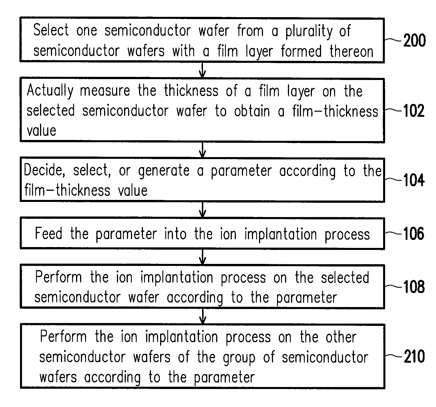
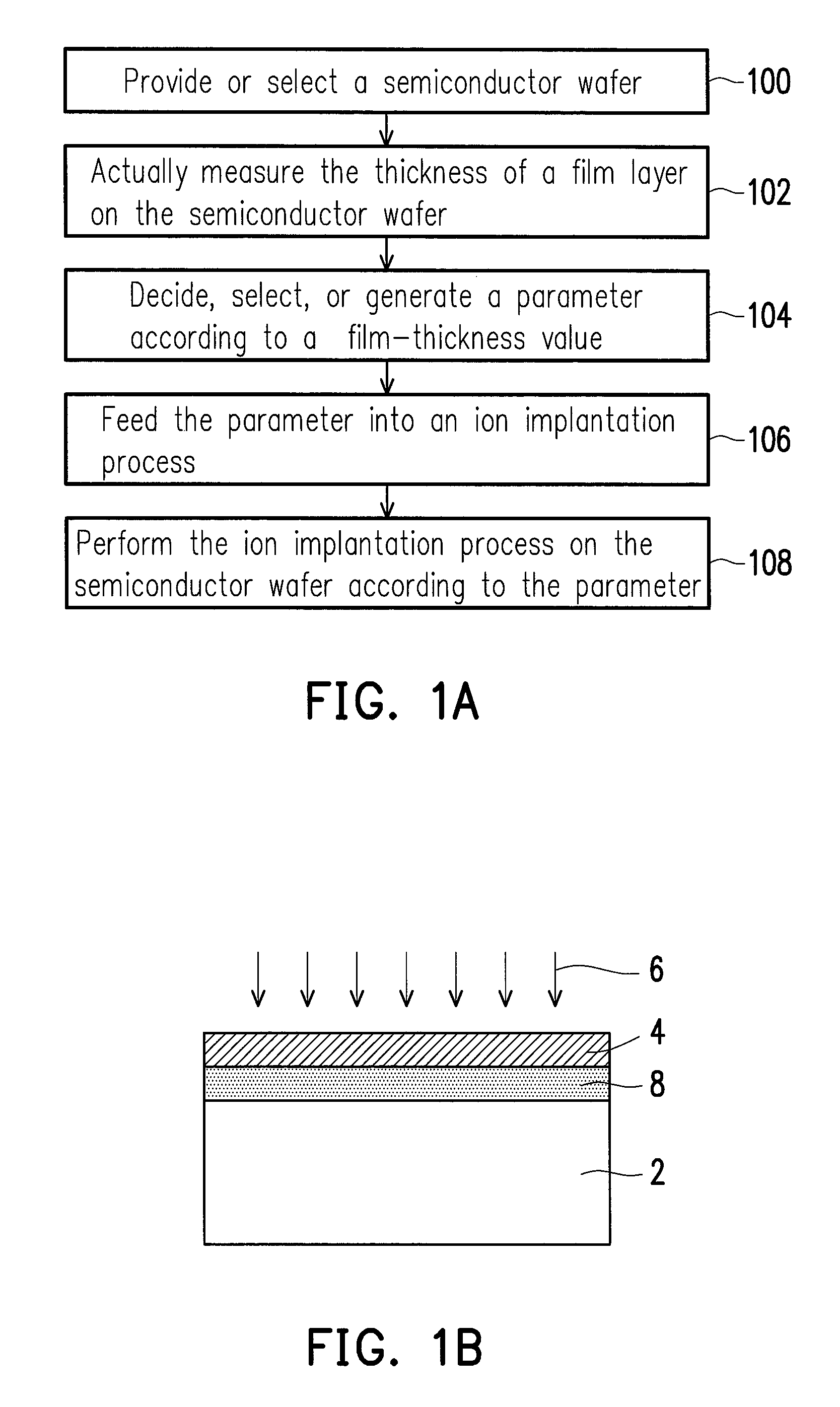
[0038]FIG. 1A is a flowchart of a method of fabricating a semiconductor device illustrated according to an embodiment of the invention. FIG. 1B is a cross-sectional diagram of a method of fabricating a semiconductor device illustrated according to an embodiment of the invention.

[0039]Referring to FIGS. 1A and 1B, in step 100, a semiconductor wafer 2 is provided or selected. A film layer 4 is formed on the semiconductor wafer 2. The film layer 4 can be a single-layer or a multi-layer. In an embodiment, the film layer 4 includes a dielectric layer or other film layers on the surface of the silicon substrate. The dielectric layer is, for instance, a silicon oxide layer. The silicon oxide layer can be a pad oxide layer or a sacrificial oxide layer. The thickness of the film layer 4 is, for instance, 10 angstroms to 300 angstroms.

[0040]Referring to FIG. 1A, in step 102, an actual measuring step of film thickness is performed on the film layer 4 on the semiconductor wafer 2 to obtain at l...


PUM


Abstract

A method of controlling a threshold voltage is provided. The method of controlling a threshold voltage includes performing a film-thickness measuring step to measure the thickness of a film layer on a wafer to obtain a film-thickness value. Then, at least one parameter is decided, selected, or generated according to the film-thickness value. Next, an ion implantation process is performed on the wafer, wherein the ion implantation process is executed according to the parameter to form a threshold voltage adjustment region in the wafer below the film layer.

Description

BACKGROUND OF THE INVENTION[0001]1. Field of the Invention[0002]The invention relates to a method of fabricating an integrated circuit, and more particularly, to a method of controlling a threshold voltage and a method of fabricating a semiconductor device.[0003]2. Description of Related Art[0004]Threshold voltage (Vt) is used for determining the reference voltage of turning on and off a transistor. In order to match the electrical properties of the various transistors in the integrated circuit with the same voltage source, the control of the threshold voltage is relatively important in the fabrication of ICs, especially to the current designs of low power and low voltage. Currently, the adjustment of the threshold voltage is done through an ion implantation process, wherein the parameter of the ion implantation is adjusted according to an empirical value and the dopant is formed on the surface of the substrate. However, the doping concentration and the uniformity of each wafer cann...

Claims


Application Information

Patent Timeline
Patent Type & Authority Patents(United States)
IPC IPC(8): H01L21/00H01L21/66H01L21/762
CPCH01L22/12H01L21/76237H01L21/76205H01L22/20
Inventor FENG, JIGU, HAI-LONGCHEN, YING-TU
Owner UNITED MICROELECTRONICS CORP
Why Eureka
Try Eureka