Organic EL element and organic EL material-containing solution

a technology of organic el and organic el, which is applied in the field of organic el devices, can solve the problems of difficult to adopt such a structure, difficult to achieve blue to green emission, and complicated manufacturing process, and achieves the effects of improving efficiency, reducing cost, and increasing device li

Active Publication Date: 2015-07-14
IDEMITSU KOSAN CO LTD
View PDF46 Cites 19 Cited by
  • Summary
  • Abstract
  • Description
  • Claims
  • Application Information

AI Technical Summary

Benefits of technology

[0020]An object of the invention is to provide an organic EL device capable of providing a mixed color by a smaller number of emitting layer(s) and having long lifetime. Also, an object of the invention is to provide an organic-EL-material-containing solution for forming the emitting layer(s) of the organic EL device.Means for Solving the Problems

Problems solved by technology

However, such a known organic EL device as disclosed in Patent Document 1 requires at least three emitting layers to be layered, which has led to complication of the manufacturing process and increase in cost.
However, it has been difficult to adopt such a structure because of the following problems.
Accordingly, the singlet energy of blue to green dopants tends to transfer to a red dopant, so that the blue to green emission is difficult to be obtained.
Hence, only the red dopant provides intense emission while blue to green emission is difficult to be obtained, so that the device as a whole will provide reddish emission.
However, these methods require minute adjustment of the doping concentrations, which would bring considerable difficulty to the manufacture of devices.
Although the problems are described above by exemplifying the fluorescent dopants that utilize the singlet energy, the same problems will be encountered when phosphorescent dopants utilizing triplet energy are used.
However, in order to secure the transfer of the triplet energy, the fluorescent-emitting layer is required to be thinned, which has led to shortening of the device lifetime.Patent Document 1: US2002 / 182441Patent Document 2: WO2006 / 038020Patent Document 3: WO2004 / 060026Non-Patent Document 1: nature vol 440 p.

Method used


Image

  • Organic EL element and organic EL material-containing solution
  • Organic EL element and organic EL material-containing solution
  • Organic EL element and organic EL material-containing solution

Examples


example 1

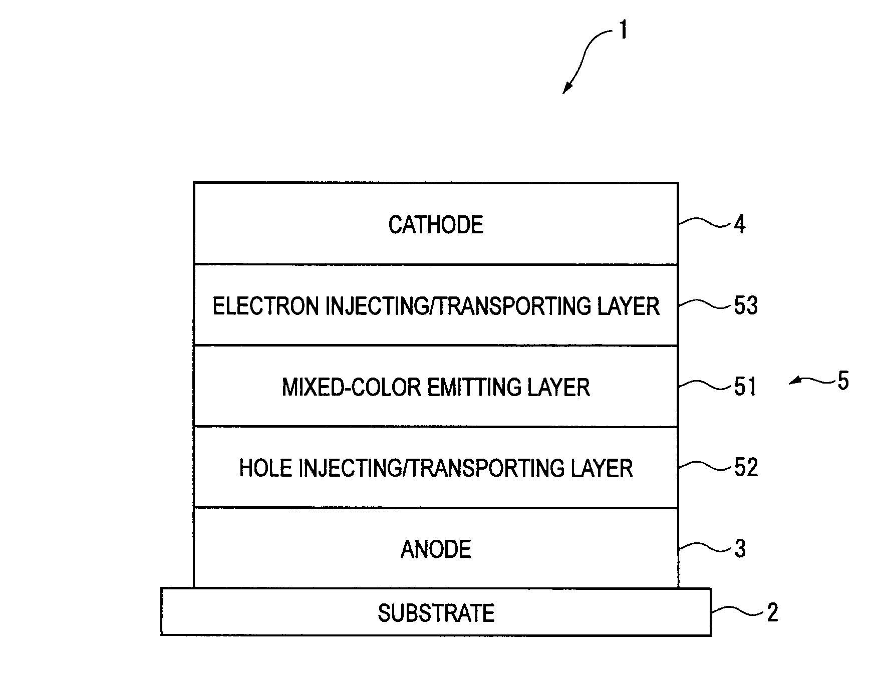
[0459]A glass substrate (size: 25 mm×75 mm×1.1 mm thick) having an ITO transparent electrode (manufactured by Geomatec Co., Ltd.) was ultrasonic-cleaned in isopropyl alcohol for five minutes, and then UV / ozone-cleaned for 30 minutes.

[0460]After the glass substrate having the transparent electrode line was cleaned, the glass substrate was mounted on a substrate holder of a vacuum deposition apparatus. Then, 55-nm thick film of 4,4′-bis[N-(1-naphthyl)-N-phenylamino]biphenyl (hereinafter abbreviated as “NPD film”) was initially formed by resistance heating deposition onto a surface of the glass substrate where the transparent electrode line was provided so that the NPD film covered the transparent electrode. The NPD film served as the hole injecting / transporting layer.

[0461]A 40-nm thick film of a compound represented by the following formula (H1) was formed on the NPD film by resistance heating deposition. At the same time, NPD and a compound represented by the following formula (RD) ...

example 2

[0466]An organic EL device was manufactured in the same manner as Example 1, except that the following compound (GD) was deposited as a green fluorescent dopant in addition to the fluorescent dopant and the red phosphorescent dopant so that the compound (GD) was contained at a content of 0.5% (mass ratio) of the compound (H1).

[0467]

example 3

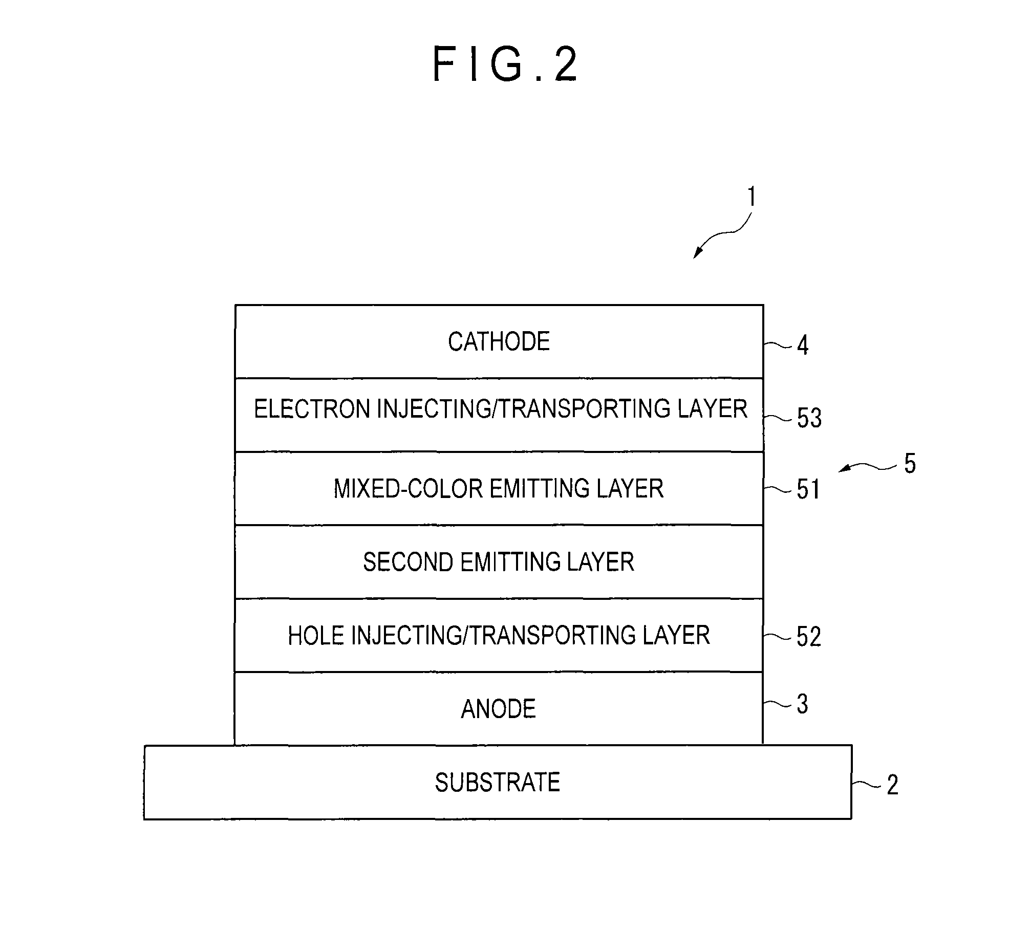
[0468]An organic EL device was manufactured in the same manner as Example 1, except that a 10-nm-thick green phosphorescent-emitting layer was provided between the mixed-color emitting layer and the hole blocking layer. The green phosphorescent-emitting layer was deposited so that Ir(ppy)3 for green phosphorescent emission was contained at a content of 5% of the CBP (i.e., host).


PUM

PropertyMeasurementUnit
triplet energy gapaaaaaaaaaa

Abstract

An organic EL device (1) includes an anode (3), a cathode (4) and an organic thin-film layer (5) provided between the anode (3) and the cathode (4). The organic thin-film layer (5) includes a single-layered mixed-color emitting layer (51) for providing mixed-color emission. The mixed-color emitting layer (51) contains a host, a fluorescent dopant for blue fluorescent emission and a phosphorescent dopant for red or green phosphorescent emission.

Description

TECHNICAL FIELD[0001]The present invention relates to an organic EL device. In particular, the invention relates to an organic EL device that provides white emission by a smaller number of emitting layer(s). The invention also relates to an organic-EL-material-containing solution for forming the emitting layer(s) of the organic EL device.BACKGROUND ART[0002]Organic EL devices are known. Such an organic EL device is a self-emitting device applicable to illuminators, displays and the like, and thus attracting more and more attentions.[0003]One of known organic EL devices includes a plurality of emitting layers that each emit light of a different wavelength. Mixture of the light emitted by the emitting layers provides mixed-color light.[0004]An example of such organic EL devices includes a layered red-emitting layer, green-emitting layer and blue-emitting layer, and provides white light in which emission from the emitting layers are mixed together (see, e.g., Patent Documents 1, 2 and ...

Claims


Application Information

Patent Timeline
Patent Type & Authority Patents(United States)
IPC IPC(8): H01L29/08H01L35/24H01L51/00H01L51/50C09K11/06C09B6/00C09B23/14C09B57/00C09B1/00C09B3/14C09B3/78
CPCH01L51/5036C09B1/00C09B3/14C09B3/78C09B6/00C09B23/148C09B57/00C09B57/008C09K11/06H01L51/0058H01L51/0072H01L51/5016C09K2211/1007C09K2211/1029C09K2211/1044H01L51/006H01L51/0061H01L51/0081H01L51/0085H10K85/626H10K85/636H10K85/633H10K85/6572H10K85/324H10K85/342H10K50/125H10K50/11H10K2101/10
Inventor NISHIMURA, KAZUKIHOSOKAWA, CHISHIOIWAKUMA, TOSHIHIROFUKUOKA, KENICHIINOUE, TETSUYA
Owner IDEMITSU KOSAN CO LTD
Why Eureka
Try Eureka