Luminescent element, preparation method thereof and luminescence method

a technology of luminescent elements and luminescent substrates, applied in the field of luminescent materials, can solve the problems of limiting the application of field emission devices, especially in the application of illumination, and low luminous efficiency, and achieves the effects of low efficiency of luminescent materials, high internal quantum efficiency of luminescent substrates, and high spontaneous emission of luminescent substrates

Inactive Publication Date: 2015-08-11
OCEANS KING LIGHTING SCI&TECH CO LTD
View PDF68 Cites 0 Cited by
  • Summary
  • Abstract
  • Description
  • Claims
  • Application Information

AI Technical Summary

Benefits of technology

[0005]In one aspect of the present disclosure, a luminescent element with a high luminescent homogeneity, high luminous efficiency, good stability, simple structure and a preparation method with a simple processes and low cost are desired.
[0006]In another aspect of the present disclosure, a luminescence method of the luminescent element with simple operation, good reliability, and high luminous efficiency is also desired.
[0015]In the luminescent element described above, the metal layer with a metal microstructure is formed on a surface of the luminescent substrate, and when irradiated by the cathode-ray, a surface plasmon can be formed between the metal layer and the luminescent substrate. Due to the surface plasmon effect, the internal quantum efficiency of the luminescent substrate is highly increased, and the spontaneous emission of the luminescent substrate is highly increased, so that the luminous efficiency of the luminescent substrate is improved and the problem of low efficiency of the luminescent materials is overcome. Accordingly, in the luminescence method of the luminescent element, once emitting cathode-ray to the metal layer, the surface plasmon will be formed between the metal layer and the luminescent substrate, thus improving the luminous efficiency and reliability. The luminescent element has a simple two-layer structure for including the luminescent substrate and the metal layer. In addition, there is a uniform interface formed between the luminescent substrate and the metal layer, so that an excellent luminescent homogeneity and stability is achieved. In the luminescence method of the luminescent element, once emitting cathode-ray to the metal layer, the surface plasmon will be formed between the metal layer and the luminescent substrate, thus improving the luminous efficiency and reliability of the luminescent substrate.
[0016]In the embodiment of the preparation method of the luminescent element, the luminescent element can be obtained by forming a metal layer on the luminescent substrate and annealing the luminescent substrate and the metal layer, thus the preparation method is simple and has a low cost and wide application prospects.

Problems solved by technology

Furthermore, materials such as the phosphor, luminescent glass, luminescent film, etc., can be served as luminescent material in field emission device, however, they all suffer from serious problems of low luminous efficiency, thus significantly limit the application of the field emission device, especially in the application of illumination.

Method used


Image

  • Luminescent element, preparation method thereof and luminescence method
  • Luminescent element, preparation method thereof and luminescence method
  • Luminescent element, preparation method thereof and luminescence method

Examples


example 1

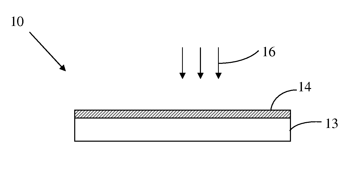
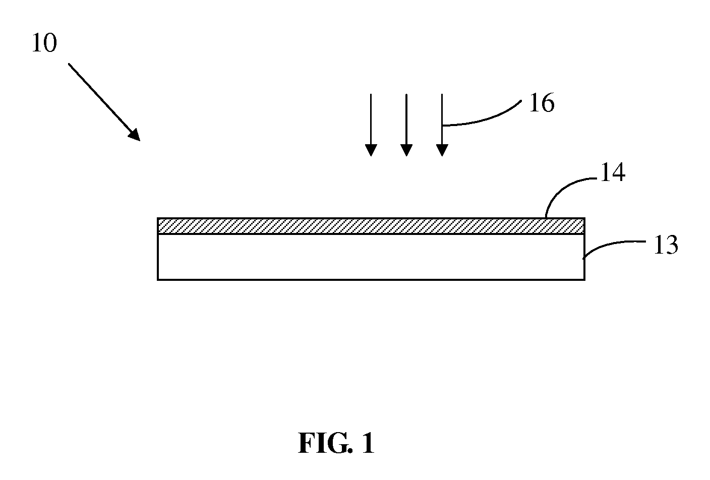
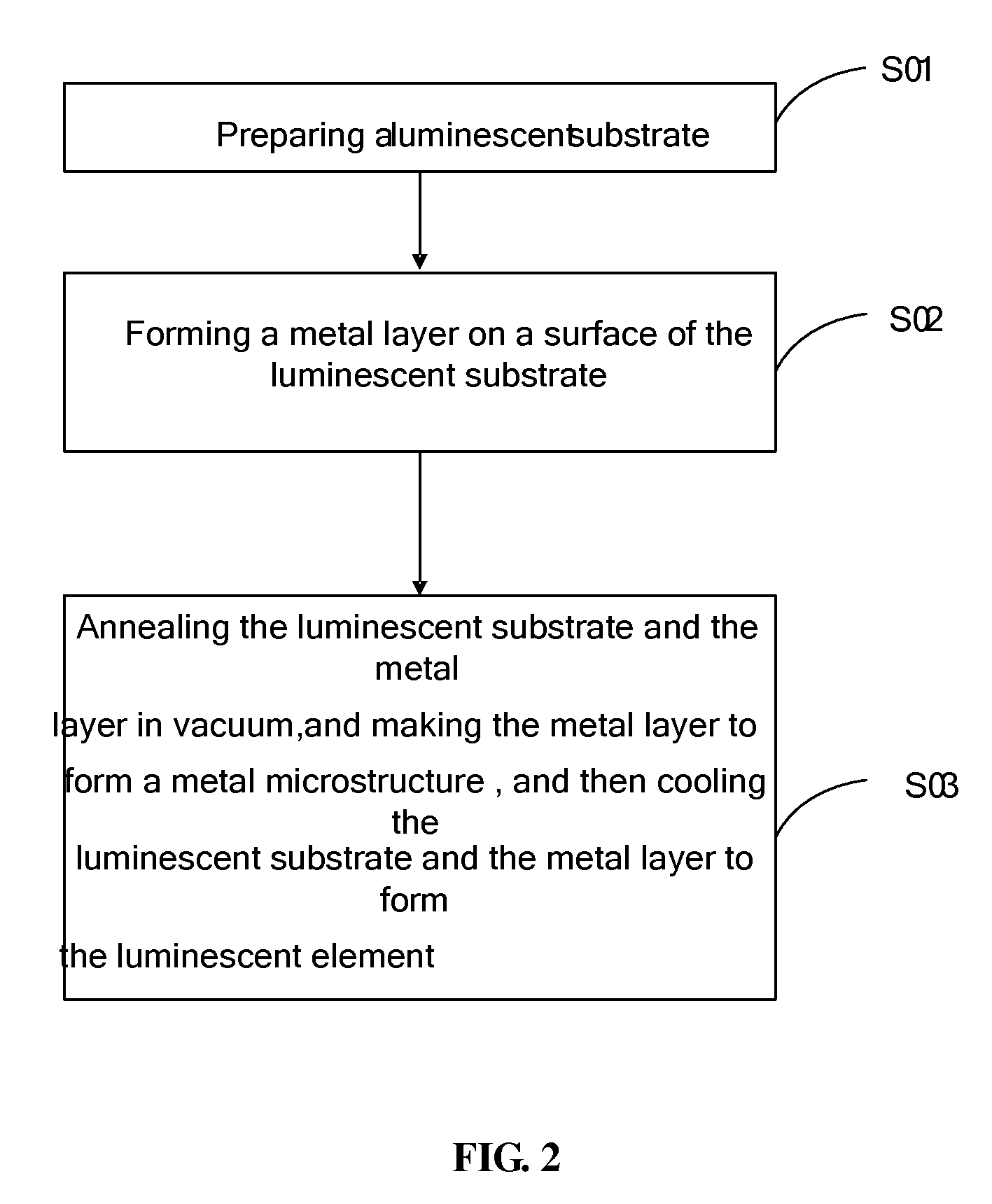
[0043]Phosphor with the composition of Y2SiO5:Tb is mixed with glass powder with the composition of 20Na2O-20BaO-30B2O3-30SiO2 in a weight ratio of 1:4, and the mixture is melt to obtain the luminescent glass doped with the luminescent material of Y2SiO5:Tb. A silver layer with a thickness of 2 nm is deposited on the surface of the luminescent glass via a magnetron sputtering equipment. The luminescent substrate and the silver layer are annealed at a temperature of 300° C. for half an hour in vacuum with the vacuum degree −3 Pa and cooled to ambient temperature, thus a luminescent element is obtained.

[0044]During the spectroscopy test, the prepared luminescent element is bombarded by cathode-ray emitted from an electron gun, and the electron beam penetrates the metal layer and irradiates the luminescent glass doped with the luminescent material of Y2SiO5:Tb, thus an emission spectrum shown in FIG. 4 is obtained, which shows that the luminescent material emits green light. In FIG. 4,...

example 2

[0046]Phosphor with the composition of Y2SiO5:Tb is mixed with glass powder with the composition of 20Na2O-20BaO-30B2O3-30SiO2 in a weight ratio of 1:19, and the mixture is melt to obtain the luminescent glass doped with the luminescent material of Y2SiO5:Tb. A gold layer with a thickness of 0.5 nm is deposited on the surface of the luminescent glass via a magnetron sputtering equipment. The luminescent substrate and the gold layer are annealed at a temperature of 200° C. for one hour in vacuum with the vacuum degree −3 Pa and cooled to ambient temperature, thus a luminescent element is obtained.

example 3

[0047]Phosphor with the composition of Y2SiO5:Tb is mixed with glass powder with the composition of 20Na2O-20BaO-30B2O3-30SiO2 in a weight ratio of 7:13, and the mixture is melt to obtain the luminescent glass doped with the luminescent material of Y2SiO5:Tb. An aluminum layer with a thickness of 200 nm is deposited on the surface of the luminescent glass via a magnetron sputtering equipment. The luminescent glass and the aluminum layer are annealed at a temperature of 500° C. for 5 hours in vacuum with the vacuum degree −3 Pa and cooled to ambient temperature, thus a luminescent element is obtained.


PUM

PropertyMeasurementUnit
temperatureaaaaaaaaaa
operating temperatureaaaaaaaaaa
weight percentaaaaaaaaaa

Abstract

A luminescent element is disclosed including: a luminescent substrate; and a metal layer with a metal microstructure formed on a surface of the luminescent substrate; wherein the luminescent substrate comprises a luminescent material with a chemical composition of Y2SiO5:Tb. A preparation method of a luminescent element and a luminescence method are also provided. The luminescent element has good luminescence homogeneity, high luminescence efficiency, good luminescence stability and simple structure, and can be used in luminescent devices with ultrahigh brightness.

Description

CROSS REFERENCE TO RELATED APPLICATIONS[0001]This application is a national stage of International Patent Application Serial No. PCT / CN2009 / 073520, filed Aug. 26, 2009, which is hereby incorporated by reference in the present disclosure in its entirety.FIELD OF THE INVENTION[0002]The present disclosure relates to luminescent materials, and more particularly relates to a luminescent element including a glass substrate made of luminescent material, preparation method thereof and luminescence method.BACKGROUND OF THE INVENTION[0003]The conventional materials used as luminescent substrate include phosphor, nanocrystal, glass, etc. Comparing to the crystal and phosphor, the glass is transparent, rigid, and has excellent chemical stability and superior luminescent performance. In addition, the glass can be easily machined into products with various shapes, such as display devices or luminescent light sources with various shapes and sizes.[0004]For example, in vacuum microelectronics, fiel...

Claims


Application Information

Patent Timeline
Patent Type & Authority Patents(United States)
IPC IPC(8): H01J23/34C03C17/09C09K11/02H01J63/04C03C4/12C09K11/77C03C3/068
CPCC03C3/068C03C4/12C03C17/09C09K11/02C09K11/7774H01J63/04C03C2218/156Y10T428/265C09K11/77742
Inventor ZHOU, MINGJIEMA, WENBOLIU, YUGANGTANG, JINGSHI, CHAOPULI, QINGTAO
Owner OCEANS KING LIGHTING SCI&TECH CO LTD
Why Eureka
Try Eureka