Substrate processing apparatus and manufacturing method for a semiconductor device

a manufacturing method and substrate technology, applied in the direction of conveyor parts, transportation and packaging, coatings, etc., can solve the problems of low production yield in the ic manufacturing method, low product quality and reliability, etc., and achieve the effect of reducing the foot print of the substrate processing apparatus

Active Publication Date: 2015-08-18
KOKUSA ELECTRIC CO LTD
View PDF13 Cites 301 Cited by
  • Summary
  • Abstract
  • Description
  • Claims
  • Application Information

AI Technical Summary

Benefits of technology

[0043]According to the above-mentioned (1), the task of maintaining the transfer chamber can be implemented via the opening section provided in a location at the rear side of the transfer chamber where the load lock chamber is not arranged, so that the passage section for allowing the worker to enter and leave and the maintenance area required on the side of the transfer chamber in installing a maintenance door on the side surface of the transfer chamber can be eliminated.
[0044]The foot print of the substrate processing apparatus can therefore be reduced. Moreover, the gate valve for the load lock chamber need not be made to a large size.

Problems solved by technology

However, a natural oxide film that might be formed on the wafer is a factor in causing lower quality and reliability of the product (IC) as well as a drop in the production yield in the IC manufacturing method.

Method used


Image

  • Substrate processing apparatus and manufacturing method for a semiconductor device
  • Substrate processing apparatus and manufacturing method for a semiconductor device
  • Substrate processing apparatus and manufacturing method for a semiconductor device

Examples


Embodiment Construction

[0049]An embodiment of the present invention is described next while referring to the accompanying drawings.

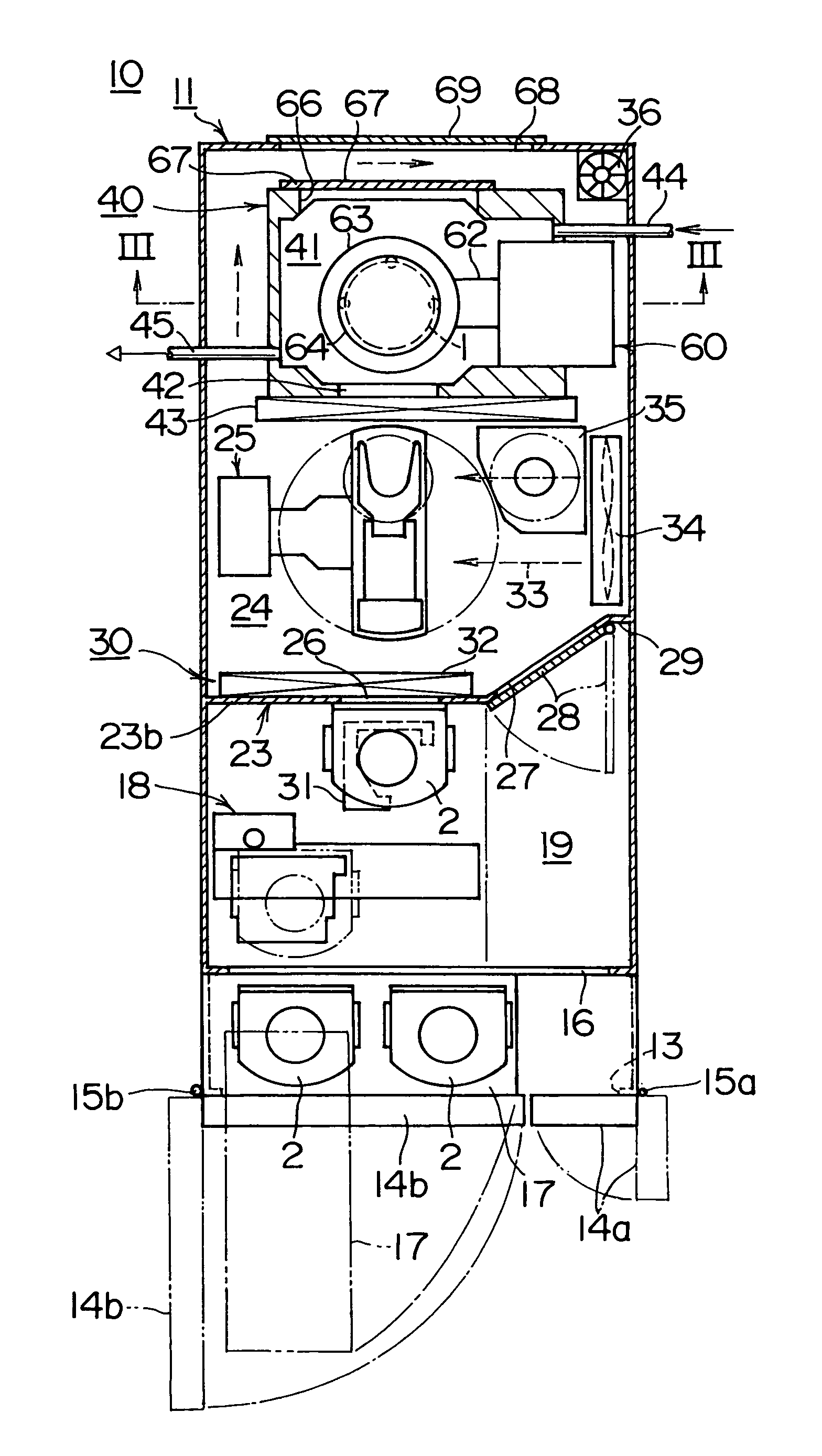
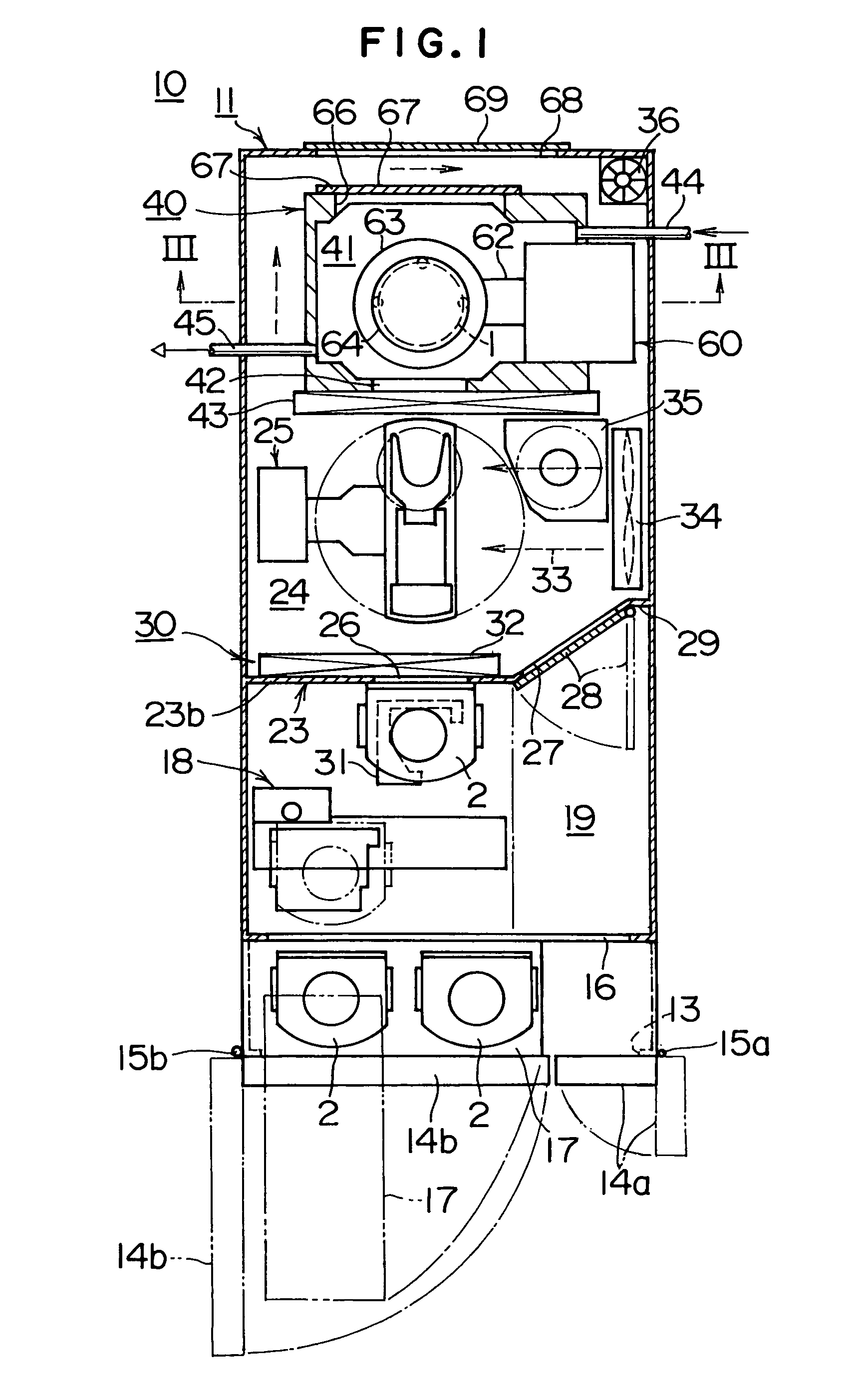
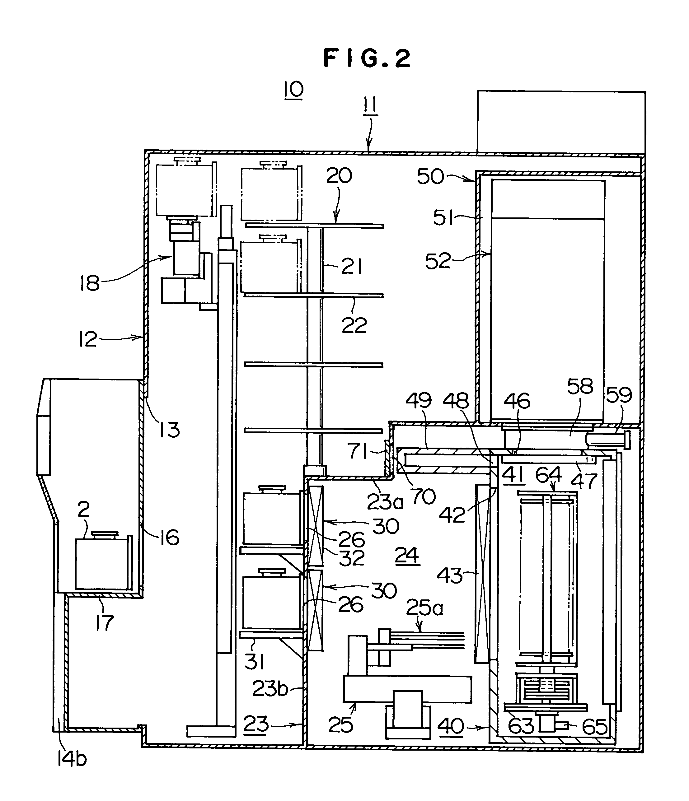
[0050]In this embodiment, the substrate processing apparatus of this invention is a batch vertical hot wall decompression CVD apparatus (hereafter called batch type CVD apparatus) used in the process of forming a CVD film such as metal film or insulating film on the wafer in the IC manufacturing method.

[0051]A batch type CVD apparatus 10 of this embodiment utilizes a FOUP (front opening unified pod, hereafter, called pod) 2 as the carrier that stores and transports wafers 1.

[0052]In the following description, the front, rear, and left, right of FIG. 1 are used as a reference. In other words, a transfer chamber 24 side is the front side, a load lock chamber 41 side is the rear side, a boat elevator 60 side is the right side, and a seal cap 63 side is the left side.

[0053]The batch type CVD apparatus 10 as shown in FIG. 1 and FIG. 2 includes a case 11 constructed in the shape of ...


PUM

PropertyMeasurementUnit
lengthaaaaaaaaaa
widthaaaaaaaaaa
Widthaaaaaaaaaa

Abstract

The sizes required for maintenance are reduced and an occupying floor area is reduced. The substrate processing apparatus contains a load lock chamber 41 and a transfer chamber 24 respectively provided in order from the rear side within a case 11; and a processing chamber 53 provided above the load lock chamber 41 for processing wafers 1. An opening section 27A, and an opening and closing means 28A for opening and closing the opening section 27A are respectively provided in a location at the rear side of the transfer chamber 24 where the load lock chamber 41 is not arranged.

Description

RELATED APPLICATIONS[0001]This application is the U.S. National Phase under 35 U.S.C. 371 of International Application No. PCT / JP2005 / 011714, filed on Jun. 27, 2005, which in turn claims the benefit of Japanese Application No. 2004-205577, filed on Jul. 13, 2004, the disclosures of which are incorporated by reference herein.TECHNICAL FIELD[0002]The present invention relates to a substrate processing apparatus and a manufacturing method for semiconductor devices, and for example, is effective for utilization in dispersing impurities into the semiconductor wafer (hereafter called, wafer) where the IC is formed and forming a CVD film such as an insulating film or metallic film on the wafer in a manufacturing method for semiconductor integrated circuit devices (hereafter called ICs).BACKGROUND ART[0003]In a factory for implementing the IC manufacturing method (hereafter called, IC manufacturing factory), the external dimensions (foot print) of the substrate processing apparatus and in p...

Claims


Application Information

Patent Timeline
Patent Type & Authority Patents(United States)
IPC IPC(8): C23C16/44H01L21/469H01L21/673H01L21/677C23C16/54H01L21/67
CPCH01L21/67303C23C16/4401C23C16/54H01L21/6773H01L21/67196H01L21/67201H01L21/22H01L21/31H01L21/68
Inventor TAKESHITA, MITSUNORIMATSUDA, TOMOYUKIHIRANO, MITSUHIROSATO, AKIHIROMORITA, SHINYAMIYATA, TOSHIMITSUSHIBATA, KOJI
Owner KOKUSA ELECTRIC CO LTD
Why Eureka
Try Eureka