
Multi pixel photo detector array of Geiger mode avalanche photodiodes

a photodiode and geiger mode technology, applied in the field of multi-pixel photo detector array of geiger mode avalanche photodiodes, can solve the problems of limiting the performance of this device, inability to localize the pixels fired by the absorption of photons, and poor spatial resolution with this techniqu

Active Publication Date: 2015-09-01
STMICROELECTRONICS SRL
View PDF5 Cites 5 Cited by
  • Summary
  • Abstract
  • Description
  • Claims
  • Application Information

AI Technical Summary

Benefits of technology

This patent describes how to make sure that information from different pixels in a camera is properly discriminated. This is done by using special photodiodes that generate different types of current pulses depending on where the light enters the camera. This information can be read by an external circuitry that connects to the camera's contacts. The technical effect of this is that it allows for better accuracy and control over the information captured by the camera.

Problems solved by technology

In a SiPM, the outputs of all the pixels are multiplexed; therefore, it is not possible to localize the pixels fired by the absorption of photons.
This drawback may limit the performance of this device and make its use possible only in applications where it is important only to determine the number of photons impinging on the detector surface, regardless of their point of absorption.
However, the spatial resolution allowed with this technique may be poor due the limited number of detectors that may be tiled together because of the complexity of the electronics, packaging constraints, the finite dimension of the same detectors required to obtain a measurable signal at their outputs, and the limited fill factor of the whole tiled array.
However, because of packaging constraints and the reduction of the fill factor due to the individual pixels outputs, arrays with a reduced number of pixels (typically 1000) may only be realized by using this approach.

Method used


Image

  • Multi pixel photo detector array of Geiger mode avalanche photodiodes
  • Multi pixel photo detector array of Geiger mode avalanche photodiodes
  • Multi pixel photo detector array of Geiger mode avalanche photodiodes

Examples


Embodiment Construction

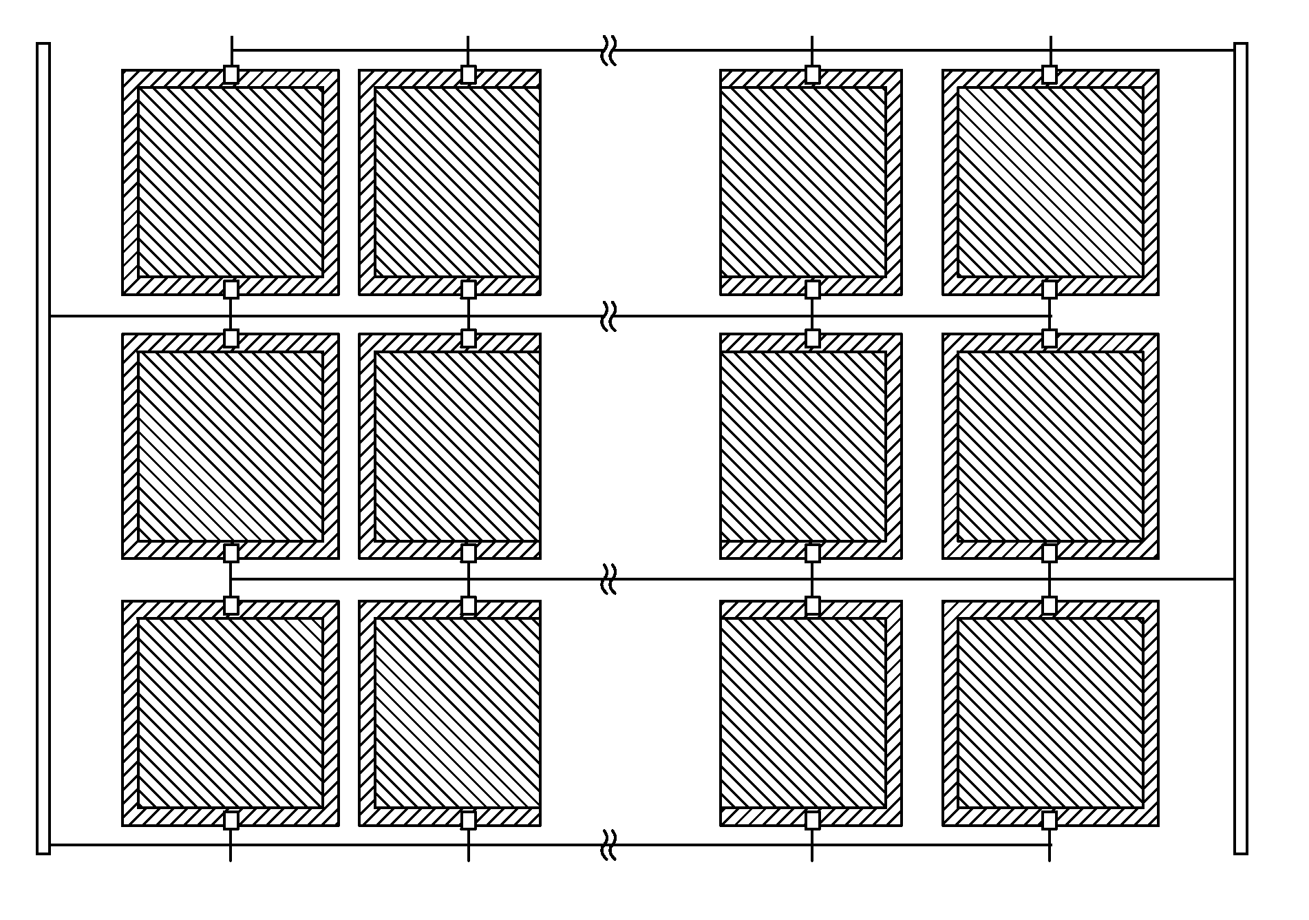
[0026]In the description herein, it is presumed that the photons impinge on only one pixel of the array at the time, i.e. only one pixel at the time is impinged by photons. In practice, it is assumed that the flux of photons has a cross-section sufficiently small to excite a single pixel.

[0027]For example, in an array of scintillation detectors, an elementary particle (e.g. a gamma ray) is absorbed by only one detector at the time. When the detector absorbs an elementary particle, it emits a photon flux usually in the visible range. By associating a pixel of the array of this disclosure to each scintillation detector, it is possible to identify the detector that has captured the elementary particle by recognizing in terms of relative intensity of response the pixel that captured the emitted photons.

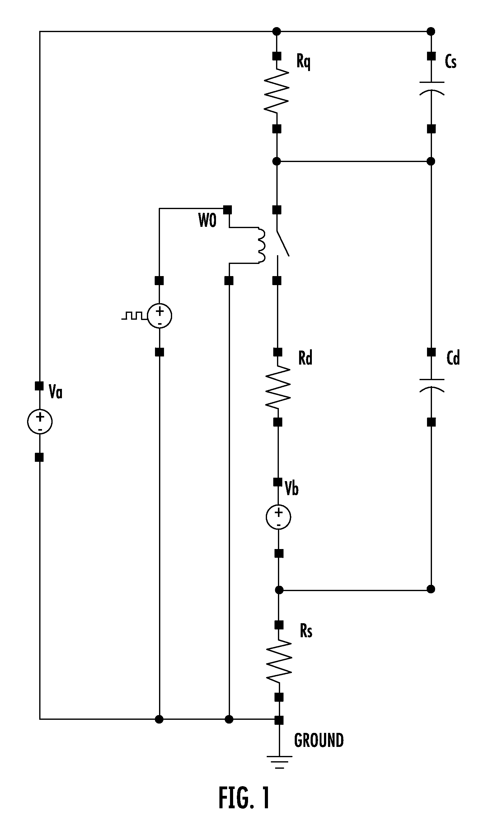
[0028]A two terminal position sensitive multi-pixel photodetector array of Geiger mode avalanche photodiodes is disclosed. According to an aspect of this disclosure, each photodiode is ch...


PUM


Abstract

A multi-pixel photodetector array may include a semiconductor substrate having a back side and a front side, Geiger mode avalanche photodiodes (GM-APDs) on the semiconductor substrate, each including an anode contact, and a common cathode for the GM-APDs and having a first connection lead on the backside of the semiconductor substrate. The multi-pixel photodetector array may include a second connection lead, and a common anode on the front side of the semiconductor substrate and configured to couple in common the anode contacts of the GM-APDs to the second connection lead. Each GM-APD may be configured to generate, when a photon impinges thereon, a current pulse of different shape for discrimination by an external circuit connected to the common cathode and the common anode.

Description

FIELD OF THE INVENTION[0001]The present disclosure relates to semiconductor photodetectors and, more precisely, to an array of Geiger-mode avalanche photodiodes.BACKGROUND OF THE INVENTION[0002]Photosensors made of semiconductor materials have gained attention in recent years because they may be specially adapted for the needs of many optical applications. See D. Renker, Properties of avalanche photodiodes for applications in high energy physics, astrophysics and medical imaging, Nuclear Instrumentation and Methods A, 486, pp. 164-169, (2002); S. Vasile, P. Gothoskar, R. Farrell and D. Sdrulla, Photon detection with high gain avalanche photodiode arrays, IEEE Transactions on Nuclear Science, 45(3), pp. 720-723, (1998); B. F. Aull, A. H. Loomis, D. J. Young, R. M. Heinrichs, B. J. Felton, P. J. Daniels, and D. J. Landers, Geiger-Mode Avalanche Photodiodes for Three-Dimensional Imaging, Lincoln Laboratory Journal, 13(2), pp. 335-350, (2002); J. C. Jackson, D. Phelan, A. P. Morrison, R...

Claims


Application Information

Patent Timeline
Patent Type & Authority Patents(United States)
IPC IPC(8): H01L31/107G01J1/46H01L27/146
CPCG01J1/46H01L27/14658H01L31/107
Inventor MAZZILLO, MASSIMO CATALDOSANFILIPPO, DELFO NUNZIATOCONDORELLI, GIOVANNI
Owner STMICROELECTRONICS SRL
Learn More