Pixel circuit, driving method thereof and pixel array structure

a pixel circuit and driving method technology, applied in the field of display techniques, can solve the problems of image sticking, variations in current, and voltage variation, and achieve the effect of reducing the charging time of the oled pixel circui

Active Publication Date: 2015-09-01
BOE TECH GRP CO LTD
View PDF8 Cites 1 Cited by
  • Summary
  • Abstract
  • Description
  • Claims
  • Application Information

AI Technical Summary

Benefits of technology

The present patent provides a pixel circuit, a driving method, and a pixel array structure that can reduce the charging time of an OLED pixel circuit. The pixel circuit includes a load controlling module, a load module, a gray scale selection module, a driving module, and a light-emitting device. The load controlling module controls the output of an analog data signal through a first node and a second node, while the load module stores the analog data signal and provides it to the driving module under the control of a first power supply. The gray scale selection module transmits a digital data signal to a third node located in the gray scale selection module under the control of a second scan signal. The driving module controls the light-emitting device under the control of the signals from the second node and the third node. The light-emitting device emits light under the actions of the second power supply and the driving module. The load module stores the analog signal, and the driving module selectively drives the light-emitting device under the control of the signals from the second node and the third node. This reduces the charging time of the OLED pixel circuit and improves the display performance.

Problems solved by technology

If the Vth in a pixel drifts as time elapses, the current would also vary with time and an image sticking may occur.
Also, the variations in the current may also be resulted from the differences in the operational voltages of the OLEDs due to the non-uniformity in the OLED devices.
Such a current-mode driving pixel circuit has a great defect in that a charging time of its capacitor is too long so that the display is affected, which may in turn restrain a large scale application of the current-mode driving circuit.

Method used


Image

  • Pixel circuit, driving method thereof and pixel array structure
  • Pixel circuit, driving method thereof and pixel array structure
  • Pixel circuit, driving method thereof and pixel array structure

Examples


first embodiment

[0065

[0066]In the present Embodiment 1, all of the thin film transistors are N-type thin film transistors TFTs which are turned on at a high level and turned off at a low level, the first power supply is a negative power supply VSS, and the second power supply is a positive power supply VDD. Optionally, the data signal line is supplied with the data signal by the semi-digitized current source. Such are similar in the following embodiments.

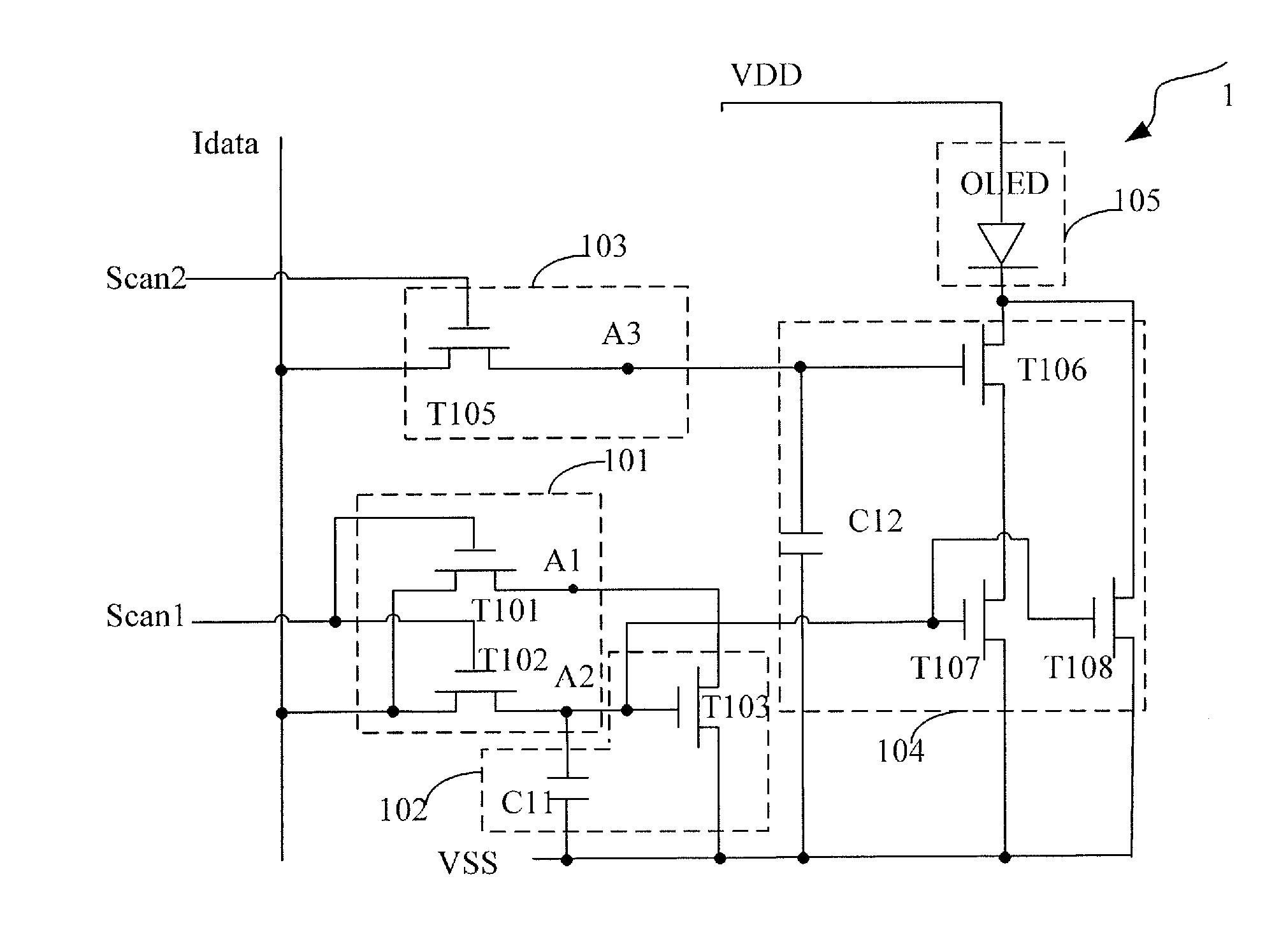
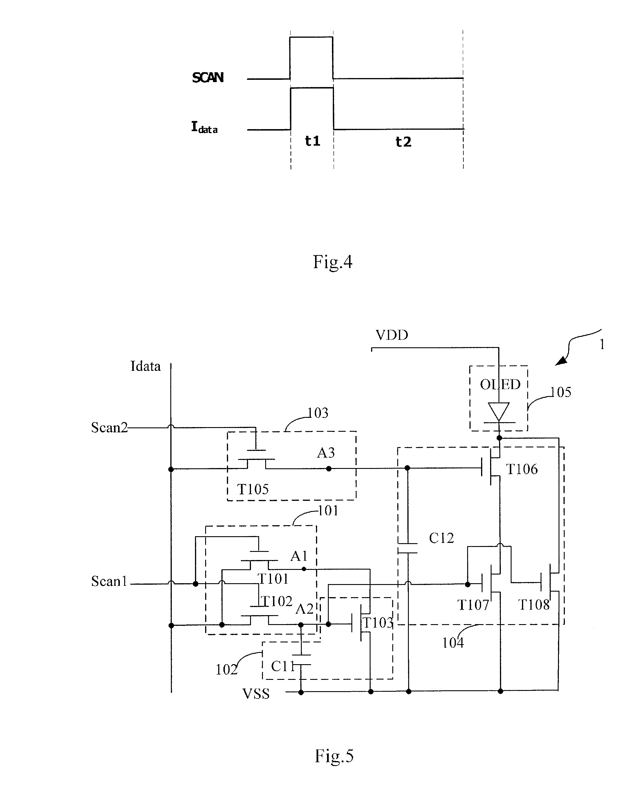
[0067]As illustrated in FIG. 5, the pixel circuit 1 according to the embodiment of the present disclosure comprises a load controlling module 101, a load module 102, a gray scale selection module 103, a driving module 104 and a light-emitting device 105, wherein:

[0068]the load controlling module 101 is connected with a first scan signal line Scan1 and a data signal line Idata, and is used for outputting an analog data signal through a first node A1 and a second node A2 under the control of a first scan signal;

[0069]the load module 102 is connected ...

second embodiment

[0095

[0096]Unlike the first Embodiment, in the second Embodiment of the present disclosure, the load module 102 may further comprise a fourth thin film transistor T104, as illustrated in FIG. 7, wherein a gate and a source of the fourth thin film transistor T104 are connected with the second power supply terminal VDD, and a drain thereof is connected with the first node A1.

[0097]Differences between a driving method according to the second Embodiment of the present disclosure and that according to the first Embodiment are in that:

[0098]during the third phase, the T104 is turned on in order to prevent the T103 from entering a deep linear region and avoid an interference with a voltage at the gate of the T103 due to a drop of a voltage at the drain of the T103, so that the T103 may be ensured to operate in a saturation region and provide the currents to the seventh thin film transistor T107 and the eighth thin film transistor T108.

[0099]Therefore the incorporation of the fourth thin fi...

third embodiment

[0101

[0102]Unlike the first Embodiment, all of the TFTs in the third Embodiment of the present disclosure are P-type TFTs which are all turned on at a low level and turned off at a high level, the first power supply is the positive power supply VDD, and the second power supply is the negative power supply VSS. A structure of the pixel circuit according to the third Embodiment is as illustrated in FIG. 9, its timing diagram is as illustrated in FIG. 10; therefore its driving method is as follows.

[0103]The driving method for the pixel circuit according to the third Embodiment of the present disclosure comprises:

[0104]During the first phase T21: the first scan signal Scan1 is at a low level, the second scan signal scan2 is at a high level, the second power supply terminal VSS outputs a high level, the data signal line Idata outputs an analog data signal, the load controlling module 101 transmits the analog data signal to the load module 102 and stores the analog data signal in the load...


PUM


Abstract

Disclosed are a pixel circuit, a driving method thereof and a pixel array structure. The pixel circuit comprises a load controlling module(101), a load module(102), a gray scale selection module(103), a driving module(104) and a light-emitting device(105). The load controlling module(101) outputs an analog data signal through a first node and a second node under the control of a first scan signal (scan1). The load module(102) is connected with a first power supply terminal(VSS), the driving module(104), the first node(A1) and the second node(A2), respectively, and stores the analog data signal in the load module(102) and provides the driving module(104) with the analog data signal under the control of signals from the first node and the second node. The gray scale selection module(103) transmits a digital data signal to a third node(A3) located in the gray scale selection module(103) under the control of a second scan signal (scan2). The driving module(104) drives the light-emitting device(105) under the control of the signals from the second node and the third node. A first terminal of the light-emitting device(105) is connected with a second power supply terminal(VDD), a second terminal thereof is connected with the driving module(104). The pixel circuit is capable of reducing a charging time of an OLED pixel circuit.

Description

TECHNICAL FIELD[0001]The present disclosure relates to a field of display technique, and particularly, to a pixel circuit, a driving method thereof and a pixel array structure.BACKGROUND[0002]The luminance of an Organic electroluminescent display OLED is directly proportional to a driving current flowing therethrough, and therefore a pixel circuit must provide the OLED with a sustained and stable driving current during a whole frame period. A driving manner of the existing OLED pixel circuit may be divided into a current driving mode and a voltage driving mode, as illustrated in FIG. 1 and FIG. 2, respectively.[0003]In a voltage-mode driving circuit, a current Ioled flowing through a light-emitting device is:[0004]IOLED=12⁢μn·Cox·WL·(Vdata-Voled-Vth)2.[0005]Wherein μn is a mobility of carriers, COX is a capacitance in an oxide layer at a gate, W / L is a width-length ratio of the transistor, Vdata is a data voltage, Voled is an operational voltage of the OLED and is shared by all of s...

Claims


Application Information

Patent Timeline
Patent Type & Authority Patents(United States)
IPC IPC(8): G09G3/30G09G3/32
CPCG09G3/3225G09G3/3241G09G2310/0262G09G2320/045
Inventor DUAN, LIYEWANG, LIRONGWU, ZHONGYUAN
Owner BOE TECH GRP CO LTD
Why Eureka
Try Eureka