Organic light emitting display and repairing method of the same

a light-emitting display and organic technology, applied in the direction of organic semiconductor devices, instruments, semiconductor devices, etc., can solve the problems of brightness deviation, brightness deviation and change, transistor may be defectiv

Active Publication Date: 2015-09-08
LG DISPLAY CO LTD
View PDF1 Cites 54 Cited by
  • Summary
  • Abstract
  • Description
  • Claims
  • Application Information

AI Technical Summary

Benefits of technology

[0022]In one or more embodiments, the terminal of the first storage capacitor is connected to the corresponding terminal of the second storage capacitor by performing welding on a repair path between the first sub-pixel and the second sub-pixel.
[0023]In one or more embodiments, the second drive transistor is connected to another terminal of the first storage capacitor and the first light emitting device.
[0024]In one or more embodiments, the second drive transistor is connected by performing ...

Problems solved by technology

During formation of each transistor included in the pixel driver, source and drain electrodes may not be separated from each other due to poor patterning of the source and drain electrodes or conductive foreign matter may remain at a thin film transistor region.
As a result, the transistor may be defective.
When current is distributed from the normal sub-p...

Method used


Image

  • Organic light emitting display and repairing method of the same
  • Organic light emitting display and repairing method of the same
  • Organic light emitting display and repairing method of the same

Examples


first embodiment

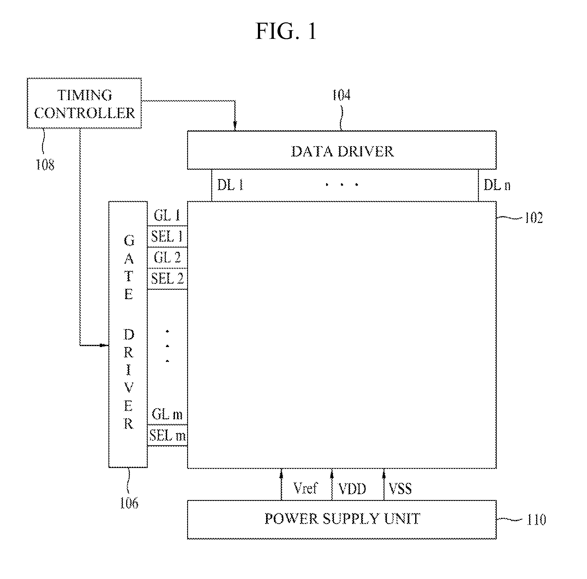
[0041]FIG. 1 is a block diagram showing an organic light emitting display according to the present invention. The organic light emitting display includes a light emitting display panel 102, a data driver 104, a gate driver 106, a timing controller 108, and a power supply unit 110.

[0042]The timing controller 108 generates a plurality of control signals to control drive timing of the gate driver 106 and the data driver 104, arranges pixel data, and supplies the pixel data to the data driver 104. The control signals generated by the timing controller 108 include a gate control signal to control drive timing of the gate driver 106 and a data control signal to control drive timing of the data driver 104.

[0043]The gate driver 106 sequentially generates a plurality of scan pulses and sensing pulses in response to the gate control signal from the timing controller 108. The gate driver 106 sequentially supplies the scan pulses to gate lines GL1 to GLm formed at the light emitting display pan...

second embodiment

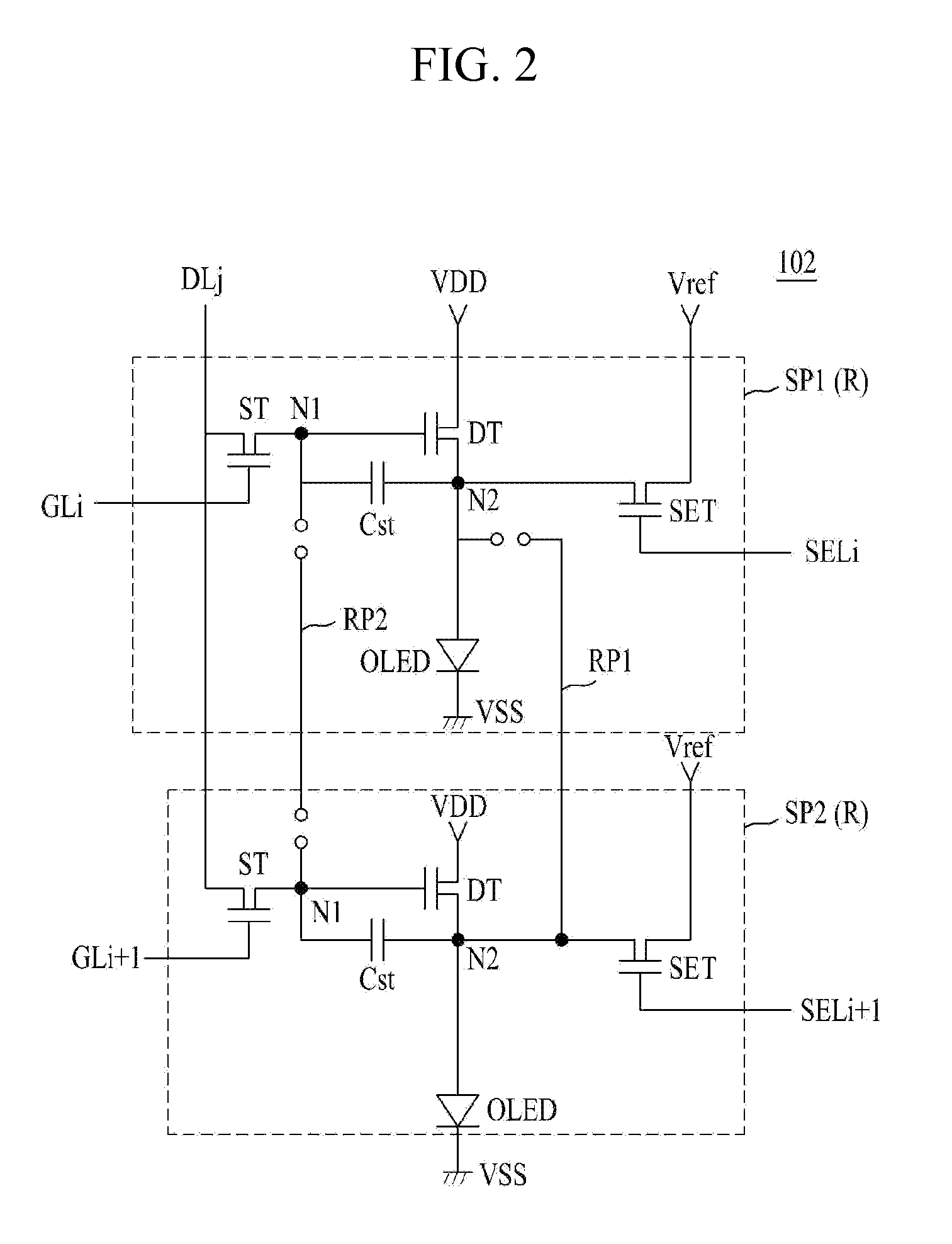
[0082]FIG. 9 is a view showing an organic light emitting display according to the present invention. The organic light emitting display shown in FIG. 9 is identical to the organic light emitting display shown in FIG. 2 except that sub-pixels embodying the same colors are arranged along a gate line. A detailed description of elements of the organic light emitting display shown in FIG. 9 identical to those of the organic light emitting display shown in FIG. 2 is omitted herein for the sake of brevity.

[0083]In the embodiment of FIG. 9, a repair pattern includes a first repair pattern RP1 formed between anodes 122 of light emitting devices OLED of horizontally adjacent sub-pixels embodying the same color and a second repair pattern RP2 formed between gate electrodes of drive transistors DT of horizontally adjacent sub-pixels.

[0084]The first repair pattern RP1 extends from an anode 122 of a normal sub-pixel adjacent to a defective sub-pixel having a defective drive transistor DT via a da...

third embodiment

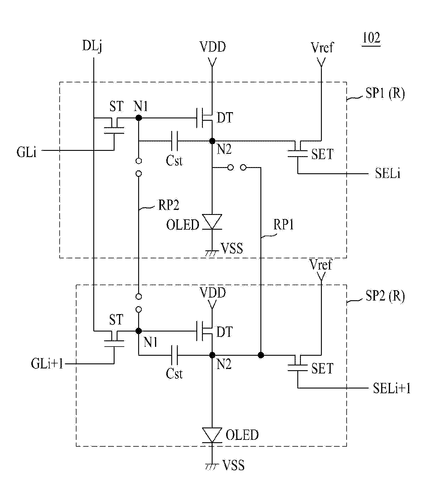
[0086]FIG. 11 is a circuit diagram showing an organic light emitting display according to the present invention. The organic light emitting display shown in FIG. 11 is identical to the organic light emitting display shown in FIG. 2 except that a repair capacitor is further provided. A detailed description of elements of the organic light emitting display shown in FIG. 11 identical to those of the organic light emitting display shown in FIG. 2 is omitted herein for the sake of brevity.

[0087]As previously described above with reference to FIG. 2, a repair pattern includes a first repair pattern RP1 formed between anodes 122 of light emitting devices OLED of vertically adjacent sub-pixels and a second repair pattern RP2 formed between gate electrodes of drive transistors DT of vertically adjacent sub-pixels embodying the same color.

[0088]In each sub-pixel, a repair capacitor RCst separate from a storage capacitor Cst is provided. When the drive transistor DT is defective, laser welding...


PUM


Abstract

A repair path is established between a sub-pixel with a defective drive transistor and another sub-pixel with an operable drive transistor to connect storage capacitors in the two sub-pixels in parallel. Another repair path is established to operate a light emitting device by the operable drive transistor of the second sub-pixel. Terminals of the storage capacitors in the two pixels are connected to a gate of the operable drive transistor. The voltage at the terminals of the storage capacitors are maintained above the threshold voltage of the operable drive transistor is switched on for a longer time due to the combined capacitance of the two storage capacitance. Hence, the sub-pixel with the defective drive transistor and the other sub-pixel of the operable drive transistor remain turned on for a longer time. Hence, despite providing a lower level of current to each of the light emitting devices in the two sub-pixels, the intensity of light produced remains relatively high due to increased turn on time of the operable drive transistor.

Description

CROSS-REFERENCE TO RELATED APPLICATION[0001]This application claims the benefit of Korean Patent Application No. 10-2014-0054743, filed on May 8, 2014, which is hereby incorporated by reference as if fully set forth herein.BACKGROUND OF THE INVENTION[0002]1. Field of the Invention[0003]The present invention relates to an organic light emitting display and a repairing method of the same and, more particularly, to an organic light emitting display with reduced brightness deviation and change over time and a repairing method of the same.[0004]2. Discussion of the Related Art[0005]Image display devices are core technology in information communication era and are used to display various kinds of information on a screen. Advancement have been made to use image display devices that are thinner, lighter, and portable and have higher performance. An organic light emitting display that controls a luminance amount of an organic emission layer to display an image has been spotlighted as a flat ...

Claims


Application Information

Patent Timeline
IPC IPC(8): H01L29/08H01L51/56H01L27/32G09G3/32
CPCH01L27/3248H01L27/3276H01L27/3211H01L51/56G09G3/3225G09G2320/0233G09G2330/08H01L2227/323G09G3/3233G09G2300/0842G09G2320/0295H10K59/123H10K59/1213H10K59/131H10K71/861
Inventor HAN, JEON-PHILLRYU, HO-JIN
Owner LG DISPLAY CO LTD
Why Eureka
Try Eureka