Light emitting element and light emitting module thereof
a technology of light emitting elements and light emitting modules, which is applied in the direction of basic electric elements, electrical equipment, semiconductor devices, etc., can solve the problems of insufficient adhesion, easy damage to devices, and breakage of wires, so as to improve heat conductivity efficiency, simplify manufacturing process, and reduce the effect of light emitting
- Summary
- Abstract
- Description
- Claims
- Application Information
AI Technical Summary
Benefits of technology
Problems solved by technology
Method used
Image


Examples
first embodiment
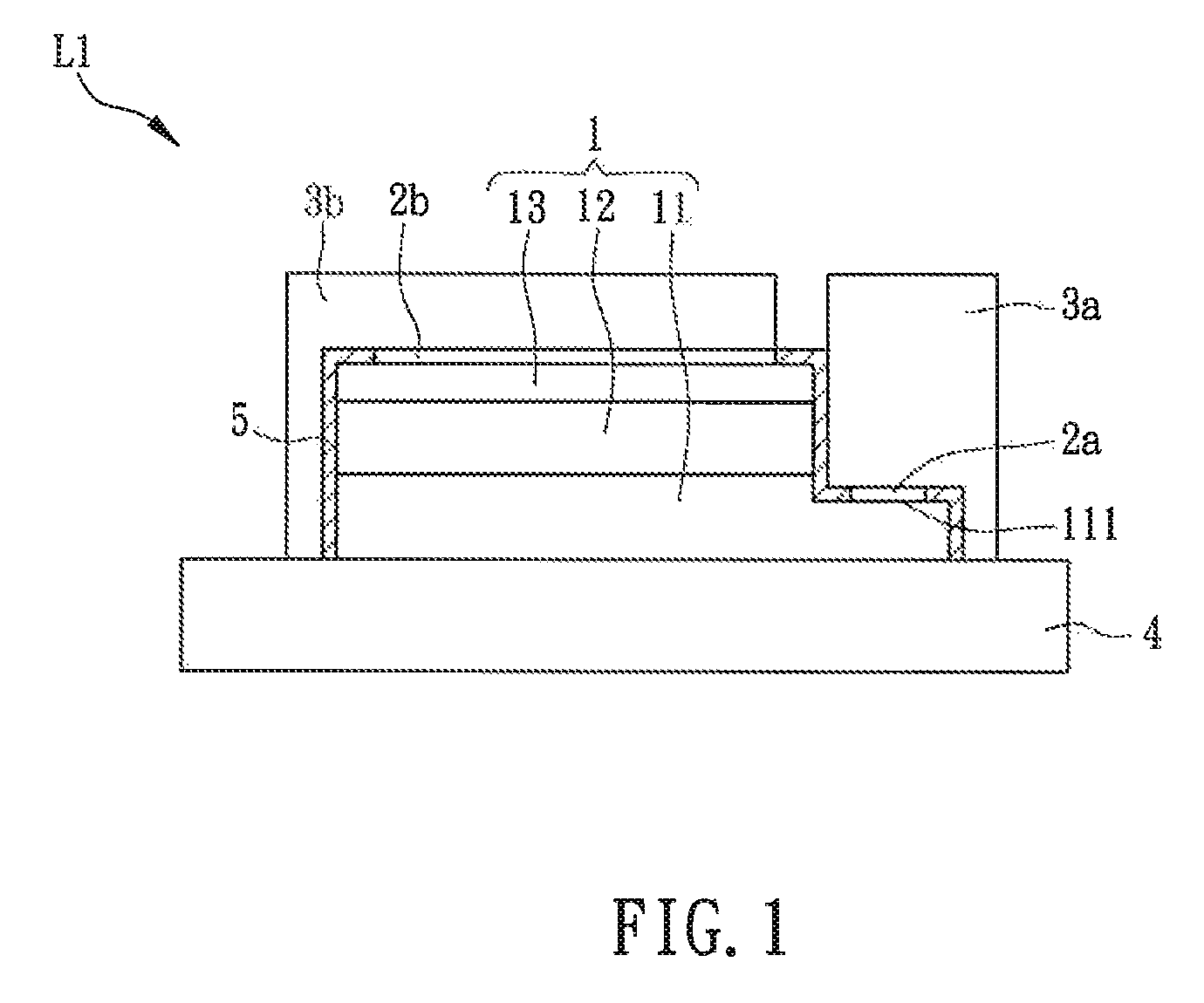
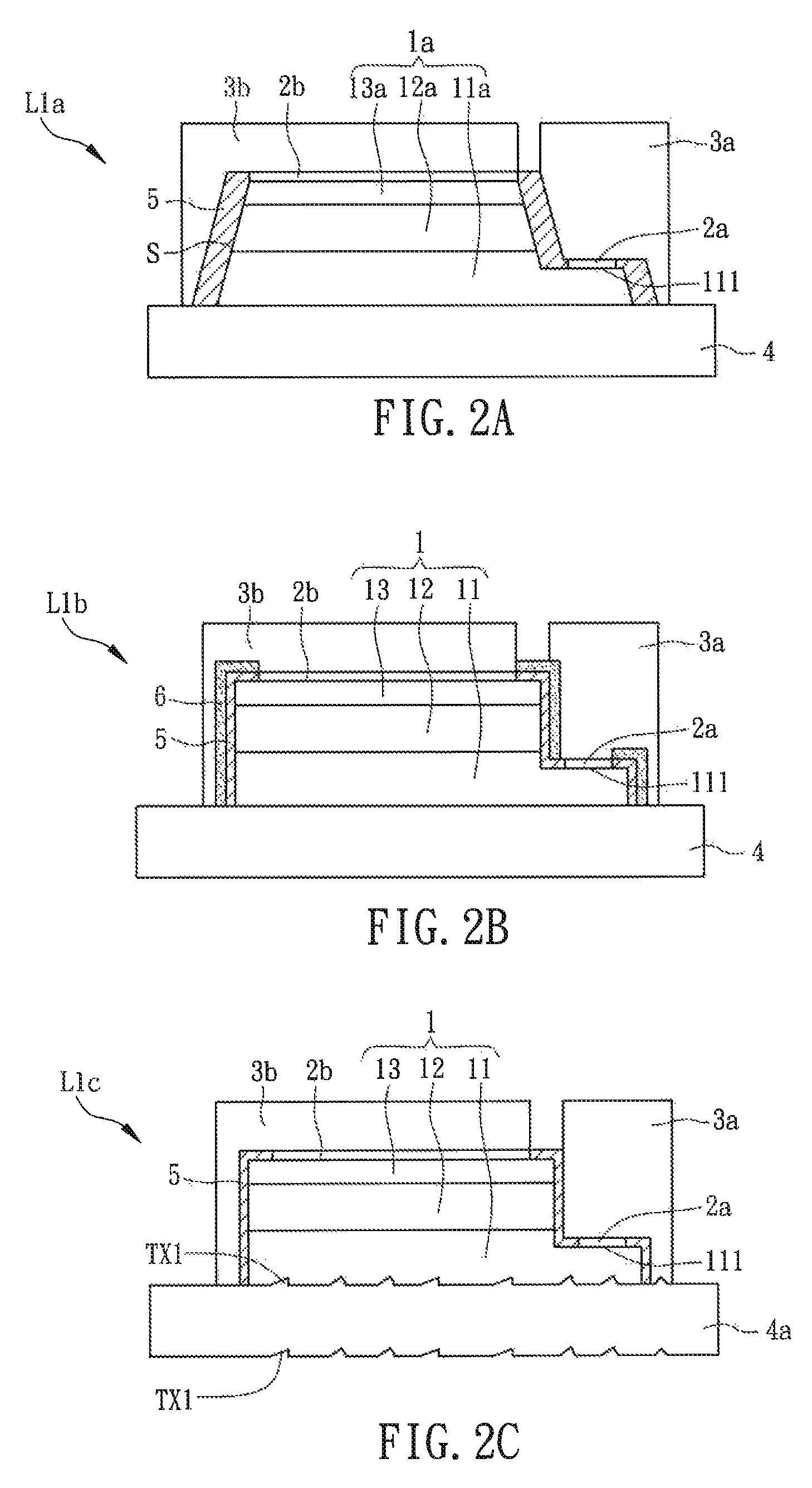
[0052]It should be noted that although each of the FIGS. 2A to 2E only show one of the aspects of the first embodiment respectively, all aspects may be implemented in the same embodiment when implementing in practice. The invention is not limited herein.
[0053]FIGS. 3A to 3D are light emitting elements according to the second preferred embodiment of the invention. Compared with FIG. 1, the light emitting element L2a shown in FIG. 3A further includes a tape T. A first bonding pad 3a and a second bonding pad 3b are disposed on the tape T. The tape T can, for example, a heat-removal tape, which adhesively fixes a portion of the structure temporarily. When heat is applied to reduce the adhesive, the portion of the structure can be removed easily to proceed with subsequent manufacturing processes. Here, the structure of the light emitting element L1 shown in FIG. 1 is taken as the basis of the subsequent variations. Of course, the aspects of the light emitting elements shown in FIGS. 2A t...
second embodiment
[0064]Compared with the light emitting element L2a of the second embodiment, the insulated substrate 4 of the light emitting element L2a is substituted by the transparent conducting layer TCL of the light emitting element L3a. Therefore, in the present embodiment, the first semiconductor layer 11c can be electrically connected by connecting at least one of the first bonding pad 3a′ to the transparent conducting layer TCL. Also, the second bonding pad 3b′ is connected to the second electrode 2b.
[0065]Although the first and the second bonding pads 3a′, 3b′ of the light emitting element L3a are both located at the same surface of the light emitting element, the electrodes, i.e. the second electrode 2b and the transparent conducting layer TCL, of the present embodiment are substantially located at different surfaces of the light emitting element L3a. Therefore, in the present embodiment, the current inside the epitaxy layer 1c passes each portion of the epitaxy layer 1c perpendicularly...
PUM
 Abstract
Description
Claims
Application Information
 - R&D
- Intellectual Property
- Life Sciences
- Materials
- Tech Scout
- Unparalleled Data Quality
- Higher Quality Content
- 60% Fewer Hallucinations
Browse by: Latest US Patents, China's latest patents, Technical Efficacy Thesaurus, Application Domain, Technology Topic, Popular Technical Reports.
© 2025 PatSnap. All rights reserved.Legal|Privacy policy|Modern Slavery Act Transparency Statement|Sitemap|About US| Contact US: help@patsnap.com